M68EVB908GB60E Freescale Semiconductor, M68EVB908GB60E Datasheet - Page 80
M68EVB908GB60E
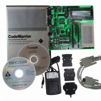
Manufacturer Part Number
M68EVB908GB60E
Description
BOARD EVAL FOR MC9S08GB60
Manufacturer
Freescale Semiconductor
Type
MCUr
Datasheet
1.M68EVB908GB60E.pdf
(290 pages)
Specifications of M68EVB908GB60E
Contents
Module and Misc Hardware
Processor To Be Evaluated
MC9S08GB
Data Bus Width
8 bit
Interface Type
RS-232
Silicon Manufacturer
Freescale
Core Architecture
HCS08
Core Sub-architecture
HCS08
Silicon Core Number
MC9S08
Silicon Family Name
S08GB
Kit Contents
GB60 Evaluation Kit
Rohs Compliant
Yes
For Use With/related Products
MC9S08GB60
Lead Free Status / RoHS Status
Lead free / RoHS Compliant


Chapter 6 Parallel Input/Output
Port A can be configured to be keyboard interrupt input pins. Refer to
(KBI)
6.3.2
Port B is an 8-bit port shared among the ATD inputs and general-purpose I/O. Any pin enabled as an ATD
input will be forced to act as an input.
Port B pins are available as general-purpose I/O pins controlled by the port B data (PTBD), data direction
(PTBDD), pullup enable (PTBPE), and slew rate control (PTBSE) registers. Refer to
I/O
When the ATD module is enabled, analog pin enables are used to specify which pins on port B will be used
as ATD inputs. Refer to
about using port B pins as ATD pins.
6.3.3
Port C is an 8-bit port which is shared among the SCI2 and IIC1 modules, and general-purpose I/O. When
SCI2 or IIC1 modules are enabled, the pin direction will be controlled by the module or function. Port C
has high current output drivers.
Port C pins are available as general-purpose I/O pins controlled by the port C data (PTCD), data direction
(PTCDD), pullup enable (PTCPE), and slew rate control (PTCSE) registers. Refer to
I/O
When the SCI2 module is enabled, PTC0 serves as the SCI2 module’s transmit pin (TxD2) and PTC1
serves as the receive pin (RxD2). Refer to
for more information about using PTC0 and PTC1 as SCI pins
When the IIC module is enabled, PTC2 serves as the IIC modules’s serial data input/output pin (SDA1)
and PTC3 serves as the clock pin (SCL1). Refer to
for more information about using PTC2 and PTC3 as IIC pins.
80
Controls,”
Controls,”
Port B
Port C
Module,”
Port B and Analog to Digital Converter Inputs
Port C and SCI2, IIC, and High-Current Drivers
for more information about general-purpose I/O control.
for more information about general-purpose I/O control.
for more information about using port A pins as keyboard interrupts pins.
MCU Pin:
MCU Pin:
Chapter 14, “Analog-to-Digital Converter (ATD)
AD1P7
PTB7/
PTC7
Bit 7
Bit 7
MC9S08GB/GT Data Sheet, Rev. 2.3
AD1P6
PTB6/
PTC6
Figure 6-3. Port B Pin Names
Figure 6-4. Port C Pin Names
6
6
Chapter 11, “Serial Communications Interface (SCI)
AD1P5
PTB5/
PTC5
5
5
Chapter 13, “Inter-Integrated Circuit (IIC)
AD1P4
PTB4/
PTC4
4
3
AD1P3
PTB3/
PTC3/
SCL1
3
3
Chapter 9, “Keyboard Interrupt
AD1P2
Module,”
PTB2/
PTC2/
SDA1
2
2
AD1P1
PTB1/
PTC1/
RxD2
for more information
Section 6.4, “Parallel
Section 6.4, “Parallel
Freescale Semiconductor
1
1
AD1P0
PTB0/
PTC0/
TxD2
Bit 0
Bit 0
Module,”
Module,”
Related parts for M68EVB908GB60E
Image
Part Number
Description
Manufacturer
Datasheet
Request
R

Part Number:
Description:
Manufacturer:
Freescale Semiconductor, Inc
Datasheet:
Part Number:
Description:
Manufacturer:
Freescale Semiconductor, Inc
Datasheet:
Part Number:
Description:
Manufacturer:
Freescale Semiconductor, Inc
Datasheet:
Part Number:
Description:
Manufacturer:
Freescale Semiconductor, Inc
Datasheet:
Part Number:
Description:
Manufacturer:
Freescale Semiconductor, Inc
Datasheet:
Part Number:
Description:
Manufacturer:
Freescale Semiconductor, Inc
Datasheet:
Part Number:
Description:
Manufacturer:
Freescale Semiconductor, Inc
Datasheet:
Part Number:
Description:
Manufacturer:
Freescale Semiconductor, Inc
Datasheet:
Part Number:
Description:
Manufacturer:
Freescale Semiconductor, Inc
Datasheet:
Part Number:
Description:
Manufacturer:
Freescale Semiconductor, Inc
Datasheet:
Part Number:
Description:
Manufacturer:
Freescale Semiconductor, Inc
Datasheet:
Part Number:
Description:
Manufacturer:
Freescale Semiconductor, Inc
Datasheet:
Part Number:
Description:
Manufacturer:
Freescale Semiconductor, Inc
Datasheet:
Part Number:
Description:
Manufacturer:
Freescale Semiconductor, Inc
Datasheet:
Part Number:
Description:
Manufacturer:
Freescale Semiconductor, Inc
Datasheet: