M68EVB908GB60E Freescale Semiconductor, M68EVB908GB60E Datasheet - Page 93
M68EVB908GB60E
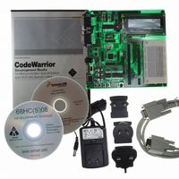
Manufacturer Part Number
M68EVB908GB60E
Description
BOARD EVAL FOR MC9S08GB60
Manufacturer
Freescale Semiconductor
Type
MCUr
Datasheet
1.M68EVB908GB60E.pdf
(290 pages)
Specifications of M68EVB908GB60E
Contents
Module and Misc Hardware
Processor To Be Evaluated
MC9S08GB
Data Bus Width
8 bit
Interface Type
RS-232
Silicon Manufacturer
Freescale
Core Architecture
HCS08
Core Sub-architecture
HCS08
Silicon Core Number
MC9S08
Silicon Family Name
S08GB
Kit Contents
GB60 Evaluation Kit
Rohs Compliant
Yes
For Use With/related Products
MC9S08GB60
Lead Free Status / RoHS Status
Lead free / RoHS Compliant


PTFPEn — Pullup Enable for Port F Bit n (n = 0–7)
PTFSEn — Slew Rate Control Enable for Port F Bit n (n = 0–7)
PTFDDn — Data Direction for Port F Bit n (n = 0–7)
6.6.7
Port G includes eight general-purpose I/O pins that are shared with BKGD/MS function and the oscillator
or external clock pins. Port G pins used as general-purpose I/O pins are controlled by the port G data
(PTGD), data direction (PTGDD), pullup enable (PTGPE), and slew rate control (PTGSE) registers.
Port pin PTG0, while in reset, defaults to the BKGD/MS pin. After the MCU is out of reset, PTG0 can be
configured to be a general-purpose output pin. When BKGD/MS takes control of PTG0, the corresponding
PTGDD, PTGPE, and PTGPSE bits are ignored.
Port pins PTG1 and PTG2 can be configured to be oscillator or external clock pins. When the oscillator
takes control of a port G pin, the corresponding PTGD, PTGDD, PTGSE, and PTGPE bits are ignored.
Reads of PTGD will return the logic value of the corresponding pin, provided PTGDD is 0.
Freescale Semiconductor
For port F pins that are inputs, these read/write control bits determine whether internal pullup devices
are enabled. For port F pins that are configured as outputs, these bits are ignored and the internal pullup
devices are disabled.
For port F pins that are outputs, these read/write control bits determine whether the slew rate controlled
outputs are enabled. For port F pins that are configured as inputs, these bits are ignored.
These read/write bits control the direction of port F pins and what is read for PTFD reads.
1 = Internal pullup device enabled.
0 = Internal pullup device disabled.
1 = Slew rate control enabled.
0 = Slew rate control disabled.
1 = Output driver enabled for port F bit n and PTFD reads return the contents of PTFDn.
0 = Input (output driver disabled) and reads return the pin value.
Port G Registers (PTGD, PTGPE, PTGSE, and PTGDD)
MC9S08GB/GT Data Sheet, Rev. 2.3
Parallel I/O Registers and Control Bits
93
Related parts for M68EVB908GB60E
Image
Part Number
Description
Manufacturer
Datasheet
Request
R

Part Number:
Description:
Manufacturer:
Freescale Semiconductor, Inc
Datasheet:
Part Number:
Description:
Manufacturer:
Freescale Semiconductor, Inc
Datasheet:
Part Number:
Description:
Manufacturer:
Freescale Semiconductor, Inc
Datasheet:
Part Number:
Description:
Manufacturer:
Freescale Semiconductor, Inc
Datasheet:
Part Number:
Description:
Manufacturer:
Freescale Semiconductor, Inc
Datasheet:
Part Number:
Description:
Manufacturer:
Freescale Semiconductor, Inc
Datasheet:
Part Number:
Description:
Manufacturer:
Freescale Semiconductor, Inc
Datasheet:
Part Number:
Description:
Manufacturer:
Freescale Semiconductor, Inc
Datasheet:
Part Number:
Description:
Manufacturer:
Freescale Semiconductor, Inc
Datasheet:
Part Number:
Description:
Manufacturer:
Freescale Semiconductor, Inc
Datasheet:
Part Number:
Description:
Manufacturer:
Freescale Semiconductor, Inc
Datasheet:
Part Number:
Description:
Manufacturer:
Freescale Semiconductor, Inc
Datasheet:
Part Number:
Description:
Manufacturer:
Freescale Semiconductor, Inc
Datasheet:
Part Number:
Description:
Manufacturer:
Freescale Semiconductor, Inc
Datasheet:
Part Number:
Description:
Manufacturer:
Freescale Semiconductor, Inc
Datasheet: