M68EVB908GB60E Freescale Semiconductor, M68EVB908GB60E Datasheet - Page 195
M68EVB908GB60E
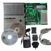
Manufacturer Part Number
M68EVB908GB60E
Description
BOARD EVAL FOR MC9S08GB60
Manufacturer
Freescale Semiconductor
Type
MCUr
Datasheet
1.M68EVB908GB60E.pdf
(290 pages)
Specifications of M68EVB908GB60E
Contents
Module and Misc Hardware
Processor To Be Evaluated
MC9S08GB
Data Bus Width
8 bit
Interface Type
RS-232
Silicon Manufacturer
Freescale
Core Architecture
HCS08
Core Sub-architecture
HCS08
Silicon Core Number
MC9S08
Silicon Family Name
S08GB
Kit Contents
GB60 Evaluation Kit
Rohs Compliant
Yes
For Use With/related Products
MC9S08GB60
Lead Free Status / RoHS Status
Lead free / RoHS Compliant


Functional Description
When CPHA = 0, the slave begins to drive its MISO output with the first data bit value (MSB or LSB
depending on LSBFE) when SS1 goes to active low. The first SPSCK edge causes both the master and the
slave to sample the data bit values on their MISO and MOSI inputs, respectively. At the second SPSCK
edge, the SPI shifter shifts one bit position which shifts in the bit value that was just sampled and shifts the
second data bit value out the other end of the shifter to the MOSI and MISO outputs of the master and
slave, respectively. When CPHA = 0, the slave’s SS input must go to its inactive high level between
transfers.
12.3.2
SPI Pin Controls
The SPI optionally shares four port pins. The function of these pins depends on the settings of SPI control
bits. When the SPI is disabled (SPE = 0), these four pins revert to being general-purpose port I/O pins that
are not controlled by the SPI.
12.3.2.1 SPSCK1 — SPI Serial Clock
When the SPI is enabled as a slave, this pin is the serial clock input. When the SPI is enabled as a master,
this pin is the serial clock output.
12.3.2.2 MOSI1 — Master Data Out, Slave Data In
When the SPI is enabled as a master and SPI pin control zero (SPC0) is 0 (not bidirectional mode), this
pin is the serial data output. When the SPI is enabled as a slave and SPC0 = 0, this pin is the serial data
input. If SPC0 = 1 to select single-wire bidirectional mode, and master mode is selected, this pin becomes
the bidirectional data I/O pin (MOMI). Also, the bidirectional mode output enable bit determines whether
the pin acts as an input (BIDIROE = 0) or an output (BIDIROE = 1). If SPC0 = 1 and slave mode is
selected, this pin is not used by the SPI and reverts to being a general-purpose port I/O pin.
12.3.2.3 MISO1 — Master Data In, Slave Data Out
When the SPI is enabled as a master and SPI pin control zero (SPC0) is 0 (not bidirectional mode), this
pin is the serial data input. When the SPI is enabled as a slave and SPC0 = 0, this pin is the serial data
output. If SPC0 = 1 to select single-wire bidirectional mode, and slave mode is selected, this pin becomes
the bidirectional data I/O pin (SISO) and the bidirectional mode output enable bit determines whether the
pin acts as an input (BIDIROE = 0) or an output (BIDIROE = 1). If SPC0 = 1 and master mode is selected,
this pin is not used by the SPI and reverts to being a general-purpose port I/O pin.
12.3.2.4 SS1 — Slave Select
When the SPI is enabled as a slave, this pin is the low-true slave select input. When the SPI is enabled as
a master and mode fault enable is off (MODFEN = 0), this pin is not used by the SPI and reverts to being
a general-purpose port I/O pin. When the SPI is enabled as a master and MODFEN = 1, the slave select
output enable bit determines whether this pin acts as the mode fault input (SSOE = 0) or as the slave select
output (SSOE = 1).
MC9S08GB/GT Data Sheet, Rev. 2.3
Freescale Semiconductor
195
Related parts for M68EVB908GB60E
Image
Part Number
Description
Manufacturer
Datasheet
Request
R

Part Number:
Description:
Manufacturer:
Freescale Semiconductor, Inc
Datasheet:
Part Number:
Description:
Manufacturer:
Freescale Semiconductor, Inc
Datasheet:
Part Number:
Description:
Manufacturer:
Freescale Semiconductor, Inc
Datasheet:
Part Number:
Description:
Manufacturer:
Freescale Semiconductor, Inc
Datasheet:
Part Number:
Description:
Manufacturer:
Freescale Semiconductor, Inc
Datasheet:
Part Number:
Description:
Manufacturer:
Freescale Semiconductor, Inc
Datasheet:
Part Number:
Description:
Manufacturer:
Freescale Semiconductor, Inc
Datasheet:
Part Number:
Description:
Manufacturer:
Freescale Semiconductor, Inc
Datasheet:
Part Number:
Description:
Manufacturer:
Freescale Semiconductor, Inc
Datasheet:
Part Number:
Description:
Manufacturer:
Freescale Semiconductor, Inc
Datasheet:
Part Number:
Description:
Manufacturer:
Freescale Semiconductor, Inc
Datasheet:
Part Number:
Description:
Manufacturer:
Freescale Semiconductor, Inc
Datasheet:
Part Number:
Description:
Manufacturer:
Freescale Semiconductor, Inc
Datasheet:
Part Number:
Description:
Manufacturer:
Freescale Semiconductor, Inc
Datasheet:
Part Number:
Description:
Manufacturer:
Freescale Semiconductor, Inc
Datasheet: