M68EVB908GB60E Freescale Semiconductor, M68EVB908GB60E Datasheet - Page 51
M68EVB908GB60E
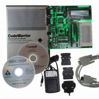
Manufacturer Part Number
M68EVB908GB60E
Description
BOARD EVAL FOR MC9S08GB60
Manufacturer
Freescale Semiconductor
Type
MCUr
Datasheet
1.M68EVB908GB60E.pdf
(290 pages)
Specifications of M68EVB908GB60E
Contents
Module and Misc Hardware
Processor To Be Evaluated
MC9S08GB
Data Bus Width
8 bit
Interface Type
RS-232
Silicon Manufacturer
Freescale
Core Architecture
HCS08
Core Sub-architecture
HCS08
Silicon Core Number
MC9S08
Silicon Family Name
S08GB
Kit Contents
GB60 Evaluation Kit
Rohs Compliant
Yes
For Use With/related Products
MC9S08GB60
Lead Free Status / RoHS Status
Lead free / RoHS Compliant


4.4.6
Block protection prevents program or erase changes for FLASH memory locations in a designated address
range. Mass erase is disabled when any block of FLASH is protected. The MC9S08GB/GT allows a block
of memory at the end of FLASH, and/or the entire FLASH memory to be block protected. A disable
control bit and a 3-bit control field, allows the user to set the size of this block. A separate control bit allows
block protection of the entire FLASH memory array. All seven of these control bits are located in the
FPROT register (see
At reset, the high-page register (FPROT) is loaded with the contents of the NVPROT location which is in
the nonvolatile register block of the FLASH memory. The value in FPROT cannot be changed directly
from application software so a runaway program cannot alter the block protection settings. If the last 512
bytes of FLASH which includes the NVPROT register is protected, the application program cannot alter
the block protection settings (intentionally or unintentionally). The FPROT control bits can be written by
background debug commands to allow a way to erase a protected FLASH memory.
One use for block protection is to block protect an area of FLASH memory for a bootloader program. This
bootloader program then can be used to erase the rest of the FLASH memory and reprogram it. Because
the bootloader is protected, it remains intact even if MCU power is lost in the middle of an erase and
reprogram operation.
Freescale Semiconductor
•
•
•
•
•
•
•
•
•
•
Writing to a FLASH address before the internal FLASH clock frequency has been set by writing
to the FCDIV register
command buffer is empty.)
Writing a second time to a FLASH address before launching the previous command (There is only
one write to FLASH for every command.)
Writing a second time to FCMD before launching the previous command (There is only one write
to FCMD for every command.)
Writing to any FLASH control register other than FCMD after writing to a FLASH address
Writing any command code other than the five allowed codes ($05, $20, $25, $40, or $41) to
FCMD
Accessing (read or write) any FLASH control register other than the write to FSTAT (to clear
FCBEF and launch the command) after writing the command to FCMD
The MCU enters stop mode while a program or erase command is in progress (The command is
aborted.)
Writing the byte program, burst program, or page erase command code ($20, $25, or $40) with a
background debug command while the MCU is secured (The background debug controller can
only do blank check and mass erase commands when the MCU is secure.)
Writing 0 to FCBEF to cancel a partial command
Writing to a FLASH address while FCBEF is not set (A new command cannot be started until the
FLASH Block Protection
Section 4.6.4, “FLASH Protection Register (FPROT and
MC9S08GB/GT Data Sheet, Rev. 2.3
NVPROT)”).
FLASH
51
Related parts for M68EVB908GB60E
Image
Part Number
Description
Manufacturer
Datasheet
Request
R

Part Number:
Description:
Manufacturer:
Freescale Semiconductor, Inc
Datasheet:
Part Number:
Description:
Manufacturer:
Freescale Semiconductor, Inc
Datasheet:
Part Number:
Description:
Manufacturer:
Freescale Semiconductor, Inc
Datasheet:
Part Number:
Description:
Manufacturer:
Freescale Semiconductor, Inc
Datasheet:
Part Number:
Description:
Manufacturer:
Freescale Semiconductor, Inc
Datasheet:
Part Number:
Description:
Manufacturer:
Freescale Semiconductor, Inc
Datasheet:
Part Number:
Description:
Manufacturer:
Freescale Semiconductor, Inc
Datasheet:
Part Number:
Description:
Manufacturer:
Freescale Semiconductor, Inc
Datasheet:
Part Number:
Description:
Manufacturer:
Freescale Semiconductor, Inc
Datasheet:
Part Number:
Description:
Manufacturer:
Freescale Semiconductor, Inc
Datasheet:
Part Number:
Description:
Manufacturer:
Freescale Semiconductor, Inc
Datasheet:
Part Number:
Description:
Manufacturer:
Freescale Semiconductor, Inc
Datasheet:
Part Number:
Description:
Manufacturer:
Freescale Semiconductor, Inc
Datasheet:
Part Number:
Description:
Manufacturer:
Freescale Semiconductor, Inc
Datasheet:
Part Number:
Description:
Manufacturer:
Freescale Semiconductor, Inc
Datasheet: