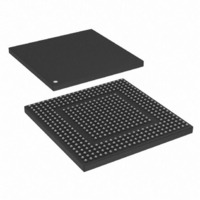
MPC8308-RDB Freescale Semiconductor, MPC8308-RDB Datasheet - Page 18

MPC8308-RDB
Manufacturer Part Number
MPC8308-RDB
Description
BOARD REF DESIGN MPC8308
Manufacturer
Freescale Semiconductor
Series
PowerQUICC II™ PROr
Type
MPUr
Datasheets
1.MPC8308VMAGD.pdf
(90 pages)
2.MPC8308VMAGD.pdf
(2 pages)
3.MPC8308-RDB.pdf
(36 pages)
4.MPC8308-RDB.pdf
(2 pages)
Specifications of MPC8308-RDB
Contents
Board, Cables, Documentation, Power Supply, Software
Ethernet Connection Type
Serial to Ethernet
Data Rate
10 Mbps, 100 Mbps, 1000 Mbps
Memory Type
DDR2, SDRAM
Interface Type
HSSI
Operating Voltage
1.5 V
Operating Current
5 uA
Maximum Power Dissipation
1000 mW
Operating Temperature Range
- 55 C to + 125 C
Product
Modules
For Use With/related Products
MPC8308
Lead Free Status / RoHS Status
Lead free / RoHS Compliant
Ethernet: Three-Speed Ethernet, MII Management
Figure 8
8.2.1.2
Table 24
18
At recommended operating conditions with LV
RX_CLK clock period 10 Mbps
RX_CLK clock period 100 Mbps
RX_CLK duty cycle
RXD[3:0], RX_DV, RX_ER setup time to RX_CLK
RXD[3:0], RX_DV, RX_ER hold time to RX_CLK
RX_CLK clock rise V
RX_CLK clock fall time V
Note:
1. The symbols used for timing specifications herein follow the pattern of t
for inputs and t
receive timing (MR) with respect to the time data input signals (D) reach the valid state (V) relative to the t
(K) going to the high (H) state or setup time. Also, t
input signals (D) went invalid (X) relative to the t
general, the clock reference symbol representation is based on three letters representing the clock of a particular functional.
For example, the subscript of t
used with the appropriate letter: R (rise) or F (fall).
shows the MII transmit AC timing diagram.
provides the MII receive AC timing specifications.
MII Receive AC Timing Specifications
(first two letters of functional block)(reference)(state)(signal)(state)
TXD[3:0]
TX_CLK
Parameter/Condition
TX_EN
TX_ER
IL
(min) to V
MPC8308 PowerQUICC II Pro Processor Hardware Specification, Rev. 2
IH
(max) to V
IH
MRX
(max)
Table 24. MII Receive AC Timing Specifications
IL
represents the MII (M) receive (RX) clock. For rise and fall times, the latter convention is
Figure 8. MII Transmit AC Timing Diagram
t
(min)
MTXH
DD
/NV
t
MTX
DD
of 3.3 V ± 0.3V.
MRX
MRDXKL
clock reference (K) going to the low (L) state or hold time. Note that, in
symbolizes MII receive timing (GR) with respect to the time data
t
t
MTKHDX
Symbol
MRXH
t
t
t
MTXF
MRDVKH
MRDXKH
t
t
t
t
MRXR
MRXF
MRX
MRX
/t
MRX
for outputs. For example, t
(first two letters of functional block)(signal)(state) (reference)(state)
1
t
MTXR
10.0
10.0
Min
1.0
1.0
35
—
—
Typ
400
40
—
—
—
—
—
MRDVKH
Freescale Semiconductor
MRX
symbolizes MII
Max
4.0
4.0
—
—
65
—
—
clock reference
Unit
ns
ns
ns
ns
ns
ns
%


