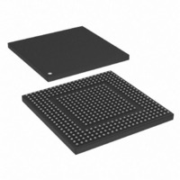
MPC8308-RDB Freescale Semiconductor, MPC8308-RDB Datasheet - Page 24

MPC8308-RDB
Manufacturer Part Number
MPC8308-RDB
Description
BOARD REF DESIGN MPC8308
Manufacturer
Freescale Semiconductor
Series
PowerQUICC II™ PROr
Type
MPUr
Datasheets
1.MPC8308VMAGD.pdf
(90 pages)
2.MPC8308VMAGD.pdf
(2 pages)
3.MPC8308-RDB.pdf
(36 pages)
4.MPC8308-RDB.pdf
(2 pages)
Specifications of MPC8308-RDB
Contents
Board, Cables, Documentation, Power Supply, Software
Ethernet Connection Type
Serial to Ethernet
Data Rate
10 Mbps, 100 Mbps, 1000 Mbps
Memory Type
DDR2, SDRAM
Interface Type
HSSI
Operating Voltage
1.5 V
Operating Current
5 uA
Maximum Power Dissipation
1000 mW
Operating Temperature Range
- 55 C to + 125 C
Product
Modules
For Use With/related Products
MPC8308
Lead Free Status / RoHS Status
Lead free / RoHS Compliant
USB
9.1.2
Table 31
Figure 13
24
USB clock cycle time
Input setup to USB clock—all inputs
Input hold to USB clock—all inputs
USB clock to output valid—all outputs
Output hold from USB clock—all outputs
Notes:
1. The symbols used for timing specifications follow the pattern of t
2. All timings are in reference to USB clock.
3. All signals are measured from NVDD/2 of the rising edge of USB clock to 0.4 × NVDD of the signal in question for 3.3-V
4. Input timings are measured at the pin.
5. For purposes of active/float timing measurements, the Hi-Z or off-state is defined to be when the total current delivered
inputs and t
(US) for the input (I) to go invalid (X) with respect to the time the usb clock reference (K) goes high (H). Also, t
symbolizes usb timing (US) for the usb clock reference (K) to go high (H), with respect to the output (O) going invalid (X) or
output hold time.
signaling levels.
through the component pin is less than or equal to the leakage current specification.
lists the general timing parameters of the USB-ULPI interface.
and
USB AC Electrical Specifications
(First two letters of functional block)(reference)(state)(signal)(state)
Output Signals
USBDR_CLK
Figure 14
Input Signals
Parameter
MPC8308 PowerQUICC II Pro Processor Hardware Specification, Rev. 2
Output
provide the AC test load and signals for the USB, respectively.
t
USKHOV
Table 31. USB General Timing Parameters
Figure 13. USB AC Test Load
Z
Figure 14. USB Signals
0
= 50 Ω
t
t
USIVKH
USKHOX
Symbol
t
t
t
t
USKHOV
USKHOX
USIVKH
USIXKH
t
USCK
(First two letters of functional block)(signal)(state)(reference)(state)
for outputs. For example, t
1
R
L
= 50 Ω
t
USIXKH
Min
15
—
4
1
1
NVDD/2
USIXKH
Max
—
—
—
—
9
Freescale Semiconductor
symbolizes usb timing
Unit
ns
ns
ns
ns
ns
USKHOX
Notes
1, 2
1, 4
1, 4
1
1
for


