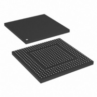
MPC8308-RDB Freescale Semiconductor, MPC8308-RDB Datasheet - Page 39

MPC8308-RDB
Manufacturer Part Number
MPC8308-RDB
Description
BOARD REF DESIGN MPC8308
Manufacturer
Freescale Semiconductor
Series
PowerQUICC II™ PROr
Type
MPUr
Datasheets
1.MPC8308VMAGD.pdf
(90 pages)
2.MPC8308VMAGD.pdf
(2 pages)
3.MPC8308-RDB.pdf
(36 pages)
4.MPC8308-RDB.pdf
(2 pages)
Specifications of MPC8308-RDB
Contents
Board, Cables, Documentation, Power Supply, Software
Ethernet Connection Type
Serial to Ethernet
Data Rate
10 Mbps, 100 Mbps, 1000 Mbps
Memory Type
DDR2, SDRAM
Interface Type
HSSI
Operating Voltage
1.5 V
Operating Current
5 uA
Maximum Power Dissipation
1000 mW
Operating Temperature Range
- 55 C to + 125 C
Product
Modules
For Use With/related Products
MPC8308
Lead Free Status / RoHS Status
Lead free / RoHS Compliant
11.4.2
The TX eye diagram in
(Figure
that must be met for the transmitter. Both diagrams must be aligned in time using the jitter median to locate
the center of the eye diagram. The different eye diagrams differ in voltage depending on whether it is a
transition bit or a de-emphasized bit. The exact reduced voltage level of the de-emphasized bit is always
relative to the transition bit.
The eye diagram must be valid for any 250 consecutive UIs.
A recovered TX UI is calculated over 3500 consecutive unit intervals of sample data. The eye diagram is
created using all edges of the 250 consecutive UI in the center of the 3500 UI used for calculating the TX
UI.
Freescale Semiconductor
Crosslink random timeout
Notes:
1. No test load is necessarily associated with this value.
2. Specified at the measurement point into a timing and voltage compliance test load as shown in
3. A T
4. The transmitter input impedance shall result in a differential return loss greater than or equal to 12 dB and a common mode
5. Measured between 20%–80% at transmitter package pins into a test load as shown in
6. See Section 4.3.1.8 of the PCI Express Base Specifications , Rev 1.0a.
7. See Section 4.2.6.3 of the PCI Express Base Specifications , Rev 1.0a.
any 250 consecutive TX UIs. (Also refer to the transmitter compliance eye diagram shown in
transmitter collected over any 250 consecutive TX UIs. The T
TX jitter budget collected over any 250 consecutive TX UIs. It should be noted that the median is not the same as the mean.
The jitter median describes the point in time where the number of jitter points on either side is approximately equal as
opposed to the averaged time value.
return loss greater than or equal to 6 dB over a frequency range of 50 MHz to 1.25 GHz. This input impedance requirement
applies to all valid input levels. The reference impedance for return loss measurements is 50 Ω to ground for both the D+ and
D– line (that is, as measured by a vector network analyzer with 50-Ω probes, see
C
TX
TX-EYE
, is optional for the return loss measurement.
Parameter
29) in place of any real PCI Express interconnect + RX component. There are two eye diagrams
= 0.70 UI provides for a total sum of deterministic and random jitter budget of T
Transmitter Compliance Eye Diagrams
It is recommended that the recovered TX UI be calculated using all edges in
the 3500 consecutive UI interval with a fit algorithm using a minimization
merit function (that is, least squares and median deviation fits).
Table 34. Differential Transmitter (TX) Output Specifications (continued)
MPC8308 PowerQUICC II Pro Processor Hardware Specification, Rev. 2
Figure 27
T
Symbol
crosslink
is specified using the passive compliance/test measurement load
This random timeout helps
resolve conflicts in
crosslink configuration by
eventually resulting in only
one Downstream and one
Upstream Port.
Comments
NOTE
TX-EYE-MEDIAN-to-MAX-JITTER
Min
0
Figure
Typical
—
Figure 29
29). Note that the series capacitors,
median is less than half of the total
TX-JITTER-MAX
Figure
Figure 29
Max
for both V
1
27.)
and measured over
= 0.30 UI for the
Units
TX-D+
ms
and V
PCI Express
Notes
TX-D-
7
39
.


