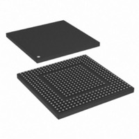
MPC8308-RDB Freescale Semiconductor, MPC8308-RDB Datasheet - Page 27

MPC8308-RDB
Manufacturer Part Number
MPC8308-RDB
Description
BOARD REF DESIGN MPC8308
Manufacturer
Freescale Semiconductor
Series
PowerQUICC II™ PROr
Type
MPUr
Datasheets
1.MPC8308VMAGD.pdf
(90 pages)
2.MPC8308VMAGD.pdf
(2 pages)
3.MPC8308-RDB.pdf
(36 pages)
4.MPC8308-RDB.pdf
(2 pages)
Specifications of MPC8308-RDB
Contents
Board, Cables, Documentation, Power Supply, Software
Ethernet Connection Type
Serial to Ethernet
Data Rate
10 Mbps, 100 Mbps, 1000 Mbps
Memory Type
DDR2, SDRAM
Interface Type
HSSI
Operating Voltage
1.5 V
Operating Current
5 uA
Maximum Power Dissipation
1000 mW
Operating Temperature Range
- 55 C to + 125 C
Product
Modules
For Use With/related Products
MPC8308
Lead Free Status / RoHS Status
Lead free / RoHS Compliant
10.2.1
Figure 16
Freescale Semiconductor
•
•
•
•
The supply voltage requirements for XCOREVDD are specified in
SerDes reference clock receiver reference circuit structure
— The SD_REF_CLK and SD_REF_CLK are internally AC-coupled differential inputs as shown
— The external reference clock driver must be able to drive this termination.
— The SerDes reference clock input can be either differential or single-ended. Refer to the
The maximum average current requirement that also determines the common mode voltage range
— When the SerDes reference clock differential inputs are DC coupled externally with the clock
— This current limitation sets the maximum common mode input voltage to be less than 0.4 V
— If the device driving the SD_REF_CLK and SD_REF_CLK inputs cannot drive 50 Ω to
The input amplitude requirement
— This requirement is described in detail in the following sections.
shows a receiver reference diagram of the SerDes reference clocks.
in
termination to XCOREVSS followed by on-chip AC-coupling.
Differential Mode and Single-ended Mode description below for further detailed requirements.
driver chip, the maximum average current allowed for each input pin is 8mA. In this case, the
exact common mode input voltage is not critical as long as it is within the range allowed by the
maximum average current of 8 mA (refer to the following bullet for more detail), since the
input is AC-coupled on-chip.
(0.4 V/50 = 8 mA) while the minimum common mode input level is 0.1 V above XCOREVSS.
For example, a clock with a 50/50 duty cycle can be produced by a clock driver with output
driven by its current source from 0mA to 16mA (0–0.8 V), such that each phase of the
differential input has a single-ended swing from 0 V to 800 mV with the common mode voltage
at 400mV.
XCOREVSS DC, or it exceeds the maximum input current limitations, then it must be
AC-coupled off-chip.
SerDes Reference Clock Receiver Characteristics
Figure
16. Each differential clock input (SD_REF_CLK or SD_REF_CLK) has a 50-Ω
MPC8308 PowerQUICC II Pro Processor Hardware Specification, Rev. 2
Figure 16. Receiver of SerDes Reference Clocks
SD_REF_CLK
SD_REF_CLK
50 Ω
50 Ω
Input
Amp
Table 1
High-Speed Serial Interfaces (HSSI)
and
Table
2.
27


