MCIMX35WPDKJ Freescale Semiconductor, MCIMX35WPDKJ Datasheet - Page 87
MCIMX35WPDKJ
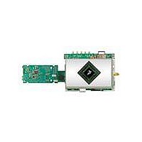
Manufacturer Part Number
MCIMX35WPDKJ
Description
BOARD DEV FOR I.MX35
Manufacturer
Freescale Semiconductor
Series
i.MX35r
Type
MPUr
Datasheets
1.MCIMX35WPDKJ.pdf
(148 pages)
2.MCIMX35WPDKJ.pdf
(2 pages)
3.MCIMX35WPDKJ.pdf
(10 pages)
Specifications of MCIMX35WPDKJ
Contents
Module and Misc Hardware
Processor To Be Evaluated
i.MX35
Processor Series
i.MX35
Data Bus Width
32 bit
Interface Type
RS-232, Ethernet, USB, CAN, JTAG
Core
ARM11
For Use With/related Products
i.MX35
Lead Free Status / RoHS Status
Lead free / RoHS Compliant


9
10
The following parameters are programmed via the DI_DISP#_TIME_CONF_1,
DI_DISP#_TIME_CONF_2, and DI_HSP_CLK_PER registers:
4.9.13.5
The IPU supports the following types of asynchronous serial interfaces:
Figure 63
DISPB_D#_CS signal and the straight polarity of the DISPB_SD_D_CLK signal.
For this interface, a bidirectional data line is used outside the device. The IPU still uses separate input and
output data lines (IPP_IND_DISPB_SD_D and IPP_DO_DISPB_SD_D). The I/O mux connects the
internal data lines to the bidirectional external line according to the IPP_OBE_DISPB_SD_D signal
provided by the IPU.
Each data transfer can be preceded by an optional preamble with programmable length and contents. The
preamble is followed by read/write (RW) and address (RS) bits. The order of the these bits is
programmable. The RW bit can be disabled. The following data can consist of one word or of a whole
burst. The interface parameters are controlled by the DI_SER_DISPn_CONF registers (n = 1, 2).
Freescale Semiconductor
Tdrp
Data read point
Loopback delay Tlbd is the cumulative propagation delay of read controls and read data. It includes an IPU output delay, a
device – level output delay, board delays, a device – level input delay, an IPU input delay. This value is device specific.
•
•
•
•
•
•
•
•
•
•
•
=
T
HSP_CLK
DISP#_IF_CLK_PER_WR, DISP#_IF_CLK_PER_RD
HSP_CLK_PERIOD
DISP#_IF_CLK_DOWN_WR
DISP#_IF_CLK_UP_WR
DISP#_IF_CLK_DOWN_RD
DISP#_IF_CLK_UP_RD
DISP#_READ_EN
3-wire (with bidirectional data line)
4-wire (with separate data input and output lines)
5-wire type 1 (with sampling RS by the serial clock)
5-wire type 2 (with sampling RS by the chip select signal)
depicts timing of the 3-wire serial interface. The timing images correspond to active-low
Serial Interfaces, Functional Description
⋅
ceil
--------------------------------------------------
HSP_CLK_PERIOD
i.MX35 Applications Processors for Industrial and Consumer Products, Rev. 9
DISP#_READ_EN
87
Related parts for MCIMX35WPDKJ
Image
Part Number
Description
Manufacturer
Datasheet
Request
R

Part Number:
Description:
MCIMX-LVDS1
Manufacturer:
Freescale Semiconductor
Datasheet:

Part Number:
Description:
Manufacturer:
Freescale Semiconductor, Inc
Datasheet:
Part Number:
Description:
Manufacturer:
Freescale Semiconductor, Inc
Datasheet:
Part Number:
Description:
Manufacturer:
Freescale Semiconductor, Inc
Datasheet:
Part Number:
Description:
Manufacturer:
Freescale Semiconductor, Inc
Datasheet:
Part Number:
Description:
Manufacturer:
Freescale Semiconductor, Inc
Datasheet:
Part Number:
Description:
Manufacturer:
Freescale Semiconductor, Inc
Datasheet:
Part Number:
Description:
Manufacturer:
Freescale Semiconductor, Inc
Datasheet:
Part Number:
Description:
Manufacturer:
Freescale Semiconductor, Inc
Datasheet:
Part Number:
Description:
Manufacturer:
Freescale Semiconductor, Inc
Datasheet:
Part Number:
Description:
Manufacturer:
Freescale Semiconductor, Inc
Datasheet:
Part Number:
Description:
Manufacturer:
Freescale Semiconductor, Inc
Datasheet:
Part Number:
Description:
Manufacturer:
Freescale Semiconductor, Inc
Datasheet:
Part Number:
Description:
Manufacturer:
Freescale Semiconductor, Inc
Datasheet:
Part Number:
Description:
Manufacturer:
Freescale Semiconductor, Inc
Datasheet: