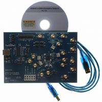
AD9549/PCBZ Analog Devices Inc, AD9549/PCBZ Datasheet - Page 20
AD9549/PCBZ
Manufacturer Part Number
AD9549/PCBZ
Description
BOARD EVALUATION FOR AD9549
Manufacturer
Analog Devices Inc
Datasheet
1.AD9549ABCPZ.pdf
(76 pages)
Specifications of AD9549/PCBZ
Main Purpose
Timing, Clock Generator
Embedded
No
Utilized Ic / Part
AD9549
Primary Attributes
2 Inputs, 2 Outputs, VCO
Secondary Attributes
CMOS, HSTL Output Logic, Graphical User Interface
Lead Free Status / RoHS Status
Lead free / RoHS Compliant


AD9549
The null points imply the existence of transmission zeros placed
at finite frequencies. While transmission zeros placed at infinity
yield minimal phase delay, zeros placed closer to dc result in
increased phase delay. Hence, the position of the first null point
has a significant impact on the phase delay introduced by the CCI
filter. This is an important consideration because excessive phase
delay negatively impacts the overall closed-loop response. As
a rule of thumb, choose a value for P so that the frequency of
the first null point (f
bandwidth or 1.5× the frequency of CLK (f
The value of P thus calculated (P
in practice. Because P is programmed as P
define P
The condition P
delay of the CCI filter on the phase margin of the loop does not
exceed 5°. P
With a properly chosen value for P, the closed-loop response of
the digital PLL is primarily determined by the response of the
digital loop filter. Flexibility in controlling the loop filter response
translates directly into flexibility in the range of applications
satisfied by the architecture of the AD9549.
The AD9549 evaluation software automatically sets the value of
the P-divider based on the user’s input criteria. Therefore, the
formulas are provided here mainly to assist in understanding
how the part works.
Direct Digital Synthesizer (DDS)
One of the primary building blocks of the digital PLL is a direct
digital synthesizer (DDS). The DDS behaves like a sinusoidal
signal generator. The frequency of the sinusoid generated by the
DDS is determined by a frequency tuning word (FTW), which
is a digital (that is, numeric) value. Unlike an analog sinusoidal
generator, a DDS uses digital building blocks and operates as a
sampled system. Thus, it requires a sampling clock (f
as the fundamental timing source of the DDS. The accumulator
behaves as a modulo-2
that is determined by the FTW. A block diagram of the DDS is
shown in Figure 25.
The input to the DDS is a 48-bit FTW that provides the
accumulator with a seed value. On each cycle of f
adds the value of the FTW to the running total of its output.
max
P
IOMAX
, 5
=
min
MAX
in terms of P
IOMAX
16
,
IO
floor
can be expressed as
≤ P
S
/P) is the greater of 80× the desired loop
IOMAX
log
48
counter with a programmable step size
IO
2
TUNING WORD
so that P
ensures that the impact of the phase
FREQUENCY
80
(FTW)
f
f
LOOP
MAX
S
IOMAX
) is the largest usable value
,
floor
can be determined.
48
48-BIT ACCUMULATOR
IO
R
/R).
, it is necessary to
log
S
, the accumulator
48
2
S
) that serves
3
48
2
f
D
f
REF
S
Figure 25. DDS Block Diagram
Q
Rev. D | Page 20 of 76
19
OFFSET
PHASE
14
19
CONVERSION
For example, given FTW = 5, the accumulator counts in
increments of 5 sec, incrementing on each f
the accumulator reaches the upper end of its capacity (2
case), at which point, it rolls over, retaining the excess. The average
rate at which the accumulator rolls over establishes the frequency of
the output sinusoid. The average rollover rate of the accumulator
is given by the following equation and establishes the output
frequency (f
Solving this equation for FTW yields
For example, given that f
FTW = 5,471,873,547,255 (0x04FA05143BF7).
The relative phase of the sinusoid can be controlled numerically,
as well. This is accomplished using the phase offset input to the
DDS (a programmable 14-bit value (Δphase); see the I/O Register
Map section). The resulting phase offset, ΔΦ (radians), is given by
The DDS can be operated in either open-loop or closed-loop
mode, via the close loop bit in the PLL control register
(Register 0x0100, Bit 0).
There are two open-loop modes: single tone and holdover. In
single-tone mode, the DDS behaves like a frequency synthesizer
and uses the value stored in the FTW0 register to determine its
output frequency. Alternatively, the FTW and Δphase values can be
determined by the device itself using the frequency estimator.
Because single-tone mode ignores the reference inputs, it is very
useful for generating test signals to aid in debugging. Single tone
mode must be activated manually via register programming.
Note that due to the internal architecture of the AD9549, the
LSB of the 48-bit tuning word becomes a don’t care when
operating the DDS in single-tone mode. This results in an
effective frequency resolution of 7 µHz with the DAC system
clock equal to 1 GHz.
AMPLITUDE
ANGLE TO
FTW
∆
f
DDS
Φ
=
=
2
=
14
DDS
π
round
∆
FTW
) of the DDS:
2
phase
48
(14-BIT)
2
DAC
14
2
f
S
48
f
S
S
= 1 GHz and f
f
DDS
f
S
I-SET
DAC+
DAC–
DDS
S
= 19.44 MHz, then
cycle. Over time,
48
in this
Related parts for AD9549/PCBZ
Image
Part Number
Description
Manufacturer
Datasheet
Request
R


Part Number:
Description:
±1.7g Dual-Axis IMEMS Accelerometer Evaluation Board
Manufacturer:
Analog Devices Inc
Datasheet:

Part Number:
Description:
Inertial Sensor Evaluation System
Manufacturer:
Analog Devices Inc
Datasheet:
Part Number:
Description:
Manufacturer:
Analog Devices Inc
Datasheet:
Part Number:
Description:
Manufacturer:
Analog Devices Inc
Datasheet:
Part Number:
Description:
Manufacturer:
Analog Devices Inc
Datasheet:
Part Number:
Description:
Manufacturer:
Analog Devices Inc
Datasheet:
Part Number:
Description:
Manufacturer:
Analog Devices Inc
Datasheet:
Part Number:
Description:
Manufacturer:
Analog Devices Inc
Datasheet:
Part Number:
Description:
Manufacturer:
Analog Devices Inc
Datasheet:
Part Number:
Description:
Manufacturer:
Analog Devices Inc
Datasheet:
Part Number:
Description:
Manufacturer:
Analog Devices Inc
Datasheet:
Part Number:
Description:
Manufacturer:
Analog Devices Inc
Datasheet: