AD9549/PCBZ Analog Devices Inc, AD9549/PCBZ Datasheet - Page 47
AD9549/PCBZ
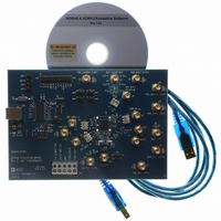
Manufacturer Part Number
AD9549/PCBZ
Description
BOARD EVALUATION FOR AD9549
Manufacturer
Analog Devices Inc
Datasheet
1.AD9549ABCPZ.pdf
(76 pages)
Specifications of AD9549/PCBZ
Main Purpose
Timing, Clock Generator
Embedded
No
Utilized Ic / Part
AD9549
Primary Attributes
2 Inputs, 2 Outputs, VCO
Secondary Attributes
CMOS, HSTL Output Logic, Graphical User Interface
Lead Free Status / RoHS Status
Lead free / RoHS Compliant


Table 12. Definitions of Terms Used in Serial Control Port Timing Diagrams
Parameter
t
t
t
t
t
t
t
t
CLK
DV
DS
DH
S
H
HI
LO
SCLK
SDIO
CSB
Description
Period of SCLK
Read data valid time (time from falling edge of SCLK to valid data on SDIO/SDO)
Setup time between data and rising edge of SCLK
Hold time between data and rising edge of SCLK
Setup time between CSB and SCLK
Hold time between CSB and SCLK
Minimum period that SCLK should be in a logic high state
Minimum period that SCLK should be in a logic low state
t
t
DS
S
BIT N
t
HI
t
DH
Figure 58. Serial Control Port Timing—Write
t
CLK
Rev. D | Page 47 of 76
t
LO
BIT N + 1
t
H
AD9549
Related parts for AD9549/PCBZ
Image
Part Number
Description
Manufacturer
Datasheet
Request
R


Part Number:
Description:
±1.7g Dual-Axis IMEMS Accelerometer Evaluation Board
Manufacturer:
Analog Devices Inc
Datasheet:

Part Number:
Description:
Inertial Sensor Evaluation System
Manufacturer:
Analog Devices Inc
Datasheet:
Part Number:
Description:
Manufacturer:
Analog Devices Inc
Datasheet:
Part Number:
Description:
Manufacturer:
Analog Devices Inc
Datasheet:
Part Number:
Description:
Manufacturer:
Analog Devices Inc
Datasheet:
Part Number:
Description:
Manufacturer:
Analog Devices Inc
Datasheet:
Part Number:
Description:
Manufacturer:
Analog Devices Inc
Datasheet:
Part Number:
Description:
Manufacturer:
Analog Devices Inc
Datasheet:
Part Number:
Description:
Manufacturer:
Analog Devices Inc
Datasheet:
Part Number:
Description:
Manufacturer:
Analog Devices Inc
Datasheet:
Part Number:
Description:
Manufacturer:
Analog Devices Inc
Datasheet:
Part Number:
Description:
Manufacturer:
Analog Devices Inc
Datasheet: