AD9549/PCBZ Analog Devices Inc, AD9549/PCBZ Datasheet - Page 73
AD9549/PCBZ
Manufacturer Part Number
AD9549/PCBZ
Description
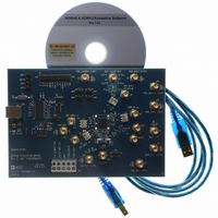
BOARD EVALUATION FOR AD9549
Manufacturer
Analog Devices Inc
Datasheet
1.AD9549ABCPZ.pdf
(76 pages)
Specifications of AD9549/PCBZ
Main Purpose
Timing, Clock Generator
Embedded
No
Utilized Ic / Part
AD9549
Primary Attributes
2 Inputs, 2 Outputs, VCO
Secondary Attributes
CMOS, HSTL Output Logic, Graphical User Interface
Lead Free Status / RoHS Status
Lead free / RoHS Compliant


APPLICATIONS INFORMATION
SAMPLE APPLICATIONS CIRCUIT
Applications Circuit Features
Features of this applications circuit include the following:
•
•
•
INPUT A
INPUT B
Input frequencies down to 8 kHz; output frequencies up to
400 MHz
Programmable loop bandwidth down to <1 Hz
Automatic redundant clock switchover with user-selectable
rate-of-phase adjustment
REF A
REF B
DIFF HSTL OUTPUT
AD9549
CMOS OUTPUT
FDBK_INB
FDBK_IN
DDS/
DAC
SYSCLK
Figure 59. AD9549 and AD9514 Precision Clock Distribution Circuit
LOW-PASS
FILTER
Rev. D | Page 73 of 76
SYNCB
CLKB
CLK
AD9514
•
•
•
•
Automatic Stratum 3/3E clock holdover, depending on the
configuration
Phase noise (f
100 Hz offset: −107 dBc/Hz; 1 kHz offset: −142 dBc/Hz;
100 kHz offset: −157 dBc/Hz; two zero-delay outputs with
programmable postdivider and synchronization
Two additional outputs (nonzero delay) on the AD9549
Programmable skew adjustment on one AD9514 output
/1...../32
/1...../32
/1...../32
C
= 122.3 MHz and 100 Hz loop bandwidth);
Δ
t
LDDS/CMOS
LVPECL
LVPECL
OUT0/
OUT0B
OUT1/
OUT1B
OUT2/
OUT2B
AD9549
Related parts for AD9549/PCBZ
Image
Part Number
Description
Manufacturer
Datasheet
Request
R


Part Number:
Description:
±1.7g Dual-Axis IMEMS Accelerometer Evaluation Board
Manufacturer:
Analog Devices Inc
Datasheet:

Part Number:
Description:
Inertial Sensor Evaluation System
Manufacturer:
Analog Devices Inc
Datasheet:
Part Number:
Description:
Manufacturer:
Analog Devices Inc
Datasheet:
Part Number:
Description:
Manufacturer:
Analog Devices Inc
Datasheet:
Part Number:
Description:
Manufacturer:
Analog Devices Inc
Datasheet:
Part Number:
Description:
Manufacturer:
Analog Devices Inc
Datasheet:
Part Number:
Description:
Manufacturer:
Analog Devices Inc
Datasheet:
Part Number:
Description:
Manufacturer:
Analog Devices Inc
Datasheet:
Part Number:
Description:
Manufacturer:
Analog Devices Inc
Datasheet:
Part Number:
Description:
Manufacturer:
Analog Devices Inc
Datasheet:
Part Number:
Description:
Manufacturer:
Analog Devices Inc
Datasheet:
Part Number:
Description:
Manufacturer:
Analog Devices Inc
Datasheet: