AD9549/PCBZ Analog Devices Inc, AD9549/PCBZ Datasheet - Page 7
AD9549/PCBZ
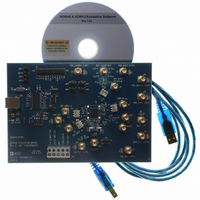
Manufacturer Part Number
AD9549/PCBZ
Description
BOARD EVALUATION FOR AD9549
Manufacturer
Analog Devices Inc
Datasheet
1.AD9549ABCPZ.pdf
(76 pages)
Specifications of AD9549/PCBZ
Main Purpose
Timing, Clock Generator
Embedded
No
Utilized Ic / Part
AD9549
Primary Attributes
2 Inputs, 2 Outputs, VCO
Secondary Attributes
CMOS, HSTL Output Logic, Graphical User Interface
Lead Free Status / RoHS Status
Lead free / RoHS Compliant


Parameter
HOLDOVER
OUTPUT FREQUENCY SLEW LIMITER
REFERENCE MONITORS
DAC OUTPUT CHARACTERISTICS
DIGITAL PLL
CMOS Output Driver
CMOS Output Driver
Frequency Accuracy
Slew Rate Resolution
Slew Rate Range
Loss of Reference Monitor
Reference Quality Monitor
Validation Timer
DCO Frequency Range (1
Output Resistance
Output Capacitance
Full-Scale Output Current
Gain Error
Output Offset
Voltage Compliance Range
Minimum Open-Loop Bandwidth
Maximum Open-Loop Bandwidth
Minimum Phase Margin
Maximum Phase Margin
PFD Input Frequency Range
Feedforward Divider Ratio
Feedback Divider Ratio
(AVDD3/Pin 37) @ 3.3 V
Frequency Range
Duty Cycle
Rise Time/Fall Time (20-80%)
(AVDD3/Pin 37) @ 1.8 V
Frequency Range
Duty Cycle
Rise Time/Fall Time (20% to 80%)
Operating Frequency Range
Minimum Frequency Error for
Minimum Frequency Error for
Maximum Frequency Error for
Maximum Frequency Error for
Operating Frequency Range
Frequency Resolution (Normalized)
Frequency Resolution (Normalized)
Timing Range
Timing Range
Continuous REF Present Indication
Continuous REF Present Indication
Continuous REF Lost Indication
Continuous REF Lost Indication
st
Nyquist Zone)
Min
0.008
45
0.008
45
0.54
0
7.63 × 10
−32
−35
0.008
0.2
408
32 × 10
65 × 10
10
−10
AVSS −
0.50
0
~0.008
1
1
−9
−6
3
Typ
55
3
55
5
50
5
20
+0.5
0.1
100
10
85
Rev. D | Page 7 of 76
Max
150
65
4.6
40
65
6.8
111
3 × 10
167 × 10
−16
−19
150
137
2.8 × 10
450
31.7
+10
0.6
AVSS +
0.50
90
~24.5
131,070
131,070
16
5
6
Unit
MHz
%
ns
MHz
%
ns
Hz/sec
Hz/sec
Hz
ppm
%
ppm
%
MHz
ppm
ppm
sec
sec
MHz
Ω
pF
mA
% FS
μA
Hz
kHz
Degrees
Degrees
MHz
Test Conditions/Comments
See
With 20 pF load and up to 150 MHz
With 20 pF load
See
With 20 pF load and up to 40 MHz
With 20 pF load
See the
P = 2
P = 2
f
f
f
f
f
divider = 1 for max (see the
Monitor
f
OOL divider = 1 for maximum
See the
P
P
DPLL loop bandwidth sets lower limit
Single-ended (each pin internally terminated to AVSS)
Range depends on DAC R
Outputs not dc-shorted to V
Dependent on the frequency of REFA/REFB, the DAC
sample rate, and the P-, R-, and S-divider values
Dependent on the frequency of REFA/REFB, the DAC
sample rate, and the P-, R-, and S-divider values
Dependent on the frequency of REFA/REFB, the DAC
sample rate, and the P-, R-, and S-divider values
Dependent on the frequency of REFA/REFB, the DAC
sample rate, and the P-, R-, and S-divider values
1, 2, …, 65,535 or 2, 4, …, 131,070
1, 2, …, 65,535 or 2, 4, …, 131,070
REF
REF
REF
REF
REF
REF
IO
IO
= 5
= 16
= 8 kHz
= 155 MHz
= 8 kHz
= 155 MHz
= 8 kHz; OOL divider = 65,535 for minimum; OOL
= 155 MHz; OOL divider = 65,535 for minimum;
Figure 14
Figure 13
16
16
for minimum; P = 2
for minimum; P = 2
Holdover
Reference Validation Timers
section)
for maximum toggle rate
for maximum toggle rate
section
SET
5
5
for maximum
for maximum
Reference Frequency
SS
resistor
section
AD9549
Related parts for AD9549/PCBZ
Image
Part Number
Description
Manufacturer
Datasheet
Request
R


Part Number:
Description:
±1.7g Dual-Axis IMEMS Accelerometer Evaluation Board
Manufacturer:
Analog Devices Inc
Datasheet:

Part Number:
Description:
Inertial Sensor Evaluation System
Manufacturer:
Analog Devices Inc
Datasheet:
Part Number:
Description:
Manufacturer:
Analog Devices Inc
Datasheet:
Part Number:
Description:
Manufacturer:
Analog Devices Inc
Datasheet:
Part Number:
Description:
Manufacturer:
Analog Devices Inc
Datasheet:
Part Number:
Description:
Manufacturer:
Analog Devices Inc
Datasheet:
Part Number:
Description:
Manufacturer:
Analog Devices Inc
Datasheet:
Part Number:
Description:
Manufacturer:
Analog Devices Inc
Datasheet:
Part Number:
Description:
Manufacturer:
Analog Devices Inc
Datasheet:
Part Number:
Description:
Manufacturer:
Analog Devices Inc
Datasheet:
Part Number:
Description:
Manufacturer:
Analog Devices Inc
Datasheet:
Part Number:
Description:
Manufacturer:
Analog Devices Inc
Datasheet: