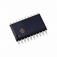
DSPIC33FJ12MC201-I/SO Microchip Technology, DSPIC33FJ12MC201-I/SO Datasheet - Page 62

DSPIC33FJ12MC201-I/SO
Manufacturer Part Number
DSPIC33FJ12MC201-I/SO
Description
IC DSPIC MCU/DSP 12K 20SOIC
Manufacturer
Microchip Technology
Series
dsPIC™ 33Fr
Datasheets
1.PIC24HJ12GP201-ISO.pdf
(84 pages)
2.DSPIC33FJ12MC201-ISO.pdf
(288 pages)
3.DSPIC33FJ12MC201-ISO.pdf
(14 pages)
4.DSPIC33FJ12MC201-IP.pdf
(284 pages)
Specifications of DSPIC33FJ12MC201-I/SO
Program Memory Type
FLASH
Program Memory Size
12KB (12K x 8)
Package / Case
20-SOIC (7.5mm Width)
Core Processor
dsPIC
Core Size
16-Bit
Speed
40 MIPs
Connectivity
I²C, IrDA, SPI, UART/USART
Peripherals
Brown-out Detect/Reset, Motor Control PWM, QEI, POR, PWM, WDT
Number Of I /o
15
Ram Size
1K x 8
Voltage - Supply (vcc/vdd)
3 V ~ 3.6 V
Data Converters
A/D 4x10b
Oscillator Type
Internal
Operating Temperature
-40°C ~ 85°C
Product
DSCs
Data Bus Width
16 bit
Processor Series
DSPIC33F
Core
dsPIC
Maximum Clock Frequency
40 MHz
Number Of Programmable I/os
15
Data Ram Size
1 KB
Maximum Operating Temperature
+ 85 C
Mounting Style
SMD/SMT
3rd Party Development Tools
52713-733, 52714-737, 53276-922, EWDSPIC
Development Tools By Supplier
PG164130, DV164035, DV244005, DV164005, PG164120, DM240001, DV164033
Minimum Operating Temperature
- 40 C
Lead Free Status / RoHS Status
Lead free / RoHS Compliant
For Use With
DV164033 - KIT START EXPLORER 16 MPLAB ICD2DM240001 - BOARD DEMO PIC24/DSPIC33/PIC32
Eeprom Size
-
Lead Free Status / Rohs Status
Lead free / RoHS Compliant
APPENDIX B:
This silicon errata issue was previously published in the
following documents, which are available from the
Microchip web site:
• dsPIC33FJXXXGPX06/X08/X10 Rev. A2 Silicon
• dsPIC33FJXXXMCX06/X08/X10 Rev. A2 Silicon
• PIC24HJXXXGPX06/X08/X10 Rev. A2 Silicon
This issue is included in this document to further assist
customers.
DS70152H-page 62
Errata (DS80306)
Errata (DS80307)
Errata (DS80280)
DEVICE ID REGISTER
SILICON ERRATA
ADDENDUM
1. Module: Device ID Register
On a few devices, the content of the Device ID
register can change from the factory programmed
default value immediately after RTSP or ICSP™
Flash programming.
As a result, development tools will not recognize
these devices and will generate an error message
indicating that the device ID and the device part
number
peripherals will be reconfigured and will not
function as described in the device data sheet.
Refer to Section 5. “Flash Programming”
(DS70191), of the “dsPIC33F Family Reference
Manual” for an explanation of RTSP and ICSP
Flash programming.
Work around
All RTSP and ICSP Flash programming routines
must be modified as follows:
1. No word programming is allowed. Any word
2. During row programming, load write latches as
3. After latches are loaded, reload any latch
4. Start
5. After row programming is complete, verify the
6. If Flash verification errors are found, repeat
Steps 1 through 5 in the work around are
implemented in MPLAB
MPLAB ICD 2, MPLAB REAL ICE™ in-circuit
emulator and MPLAB PM3 tools.
programming must be replaced with row
programming.
described in 5.4.2.3 “Loading Write Latches”
of
(DS70191).
location (in a given row) that has 5 LSB set to
0x18, with the original data. For example,
reload one of the following latch locations with
the desired data:
0xXXXX18, 0xXXXX38, 0xXXXX58,
0xXXXX78, 0xXXXX98, 0xXXXXB8,
0xXXXXD8, 0xXXXXF8
NVMOP<3:0> = ‘0001’ (Memory row program
operation) in the NVMCON register.
contents of Flash memory.
steps 2 through 5. If Flash verification errors
are found after a second iteration, report this
problem to Microchip.
Section
do
row
not
5.
© 2010 Microchip Technology Inc.
programming
match.
®
“Flash
IDE version 7.61 for the
Additionally,
Programming”
by
setting
some


