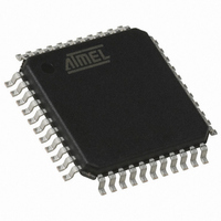
AT89C51IC2-RLTIL Atmel, AT89C51IC2-RLTIL Datasheet - Page 108

AT89C51IC2-RLTIL
Manufacturer Part Number
AT89C51IC2-RLTIL
Description
IC 8051 MCU FLASH 32K 44VQFP
Manufacturer
Atmel
Series
89Cr
Datasheet
1.AT89C51IC2-SLRIM.pdf
(147 pages)
Specifications of AT89C51IC2-RLTIL
Core Processor
8051
Core Size
8-Bit
Speed
40MHz
Connectivity
I²C, SPI, UART/USART
Peripherals
POR, PWM, WDT
Number Of I /o
34
Program Memory Size
32KB (32K x 8)
Program Memory Type
FLASH
Ram Size
1.25K x 8
Voltage - Supply (vcc/vdd)
2.7 V ~ 3.6 V
Oscillator Type
External
Operating Temperature
-40°C ~ 85°C
Package / Case
44-TQFP, 44-VQFP
Lead Free Status / RoHS Status
Contains lead / RoHS non-compliant
Eeprom Size
-
Data Converters
-
Available stocks
Company
Part Number
Manufacturer
Quantity
Price
Company:
Part Number:
AT89C51IC2-RLTIL
Manufacturer:
ATMEL
Quantity:
640
Company:
Part Number:
AT89C51IC2-RLTIL
Manufacturer:
ATMEL
Quantity:
4 116
Flash Registers and
Memory Map
Hardware Register
Flash Memory Lock Bits
108
AT89C51IC2
The AT89C51IC2 Flash memory uses several registers for its management:
•
•
The only hardware register of the AT89C51IC2 is called Hardware Security Byte (HSB).
Table 84. Hardware Security Byte (HSB)
Boot Loader Jump Bit (BLJB)
One bit of the HSB, the BLJB bit, is used to force the boot address:
•
•
The three lock bits provide different levels of protection for the on-chip code and data,
when programmed as shown in Table 85.
Number
Bit
2-0
Hardware registers can only be accessed through the parallel programming modes
which are handled by the parallel programmer.
Software registers are in a special page of the Flash memory which can be
accessed through the API or with the parallel programming modes. This page,
called "Extra Flash Memory", is not in the internal Flash program memory
addressing space.
When this bit is programmed (‘1’ value) the boot address is 0000h.
When this bit is unprogrammed (‘1’ value) the boot address is F800h. By default,
this bit is unprogrammed and the ISP is enabled.
X2
7
6
5
4
3
7
Mnemonic
XRAM
LB2-0
BLJB
OSC
BLJB
Bit
X2
-
6
Description
X2 Mode
Programmed (‘0’ value) to force X2 mode (6 clocks per instruction) after reset.
Unprogrammed (‘1’ Value) to force X1 mode, Standard Mode, after reset
(Default).
Boot Loader Jump Bit
Unprogrammed (‘1’ value) to start the user’s application on next reset at address
0000h.
Programmed (‘0’ value) to start the boot loader at address F800h on next reset
(Default).
Oscillator Bit
Programmed to allow oscillator B at startup
Unprogrammed this bit to allow oscillator A at startup ( Default).
Reserved
XRAM config bit (only programmable by programmer tools)
Programmed to inhibit XRAM
Unprogrammed, this bit to valid XRAM (Default)
User Memory Lock Bits (only programmable by programmer tools)
See Table 85
OSC
5
4
-
XRAM
3
LB2
2
LB1
1
4301D–8051–02/08
LB0
0


