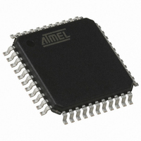
AT89C51IC2-RLTIL Atmel, AT89C51IC2-RLTIL Datasheet - Page 74

AT89C51IC2-RLTIL
Manufacturer Part Number
AT89C51IC2-RLTIL
Description
IC 8051 MCU FLASH 32K 44VQFP
Manufacturer
Atmel
Series
89Cr
Datasheet
1.AT89C51IC2-SLRIM.pdf
(147 pages)
Specifications of AT89C51IC2-RLTIL
Core Processor
8051
Core Size
8-Bit
Speed
40MHz
Connectivity
I²C, SPI, UART/USART
Peripherals
POR, PWM, WDT
Number Of I /o
34
Program Memory Size
32KB (32K x 8)
Program Memory Type
FLASH
Ram Size
1.25K x 8
Voltage - Supply (vcc/vdd)
2.7 V ~ 3.6 V
Oscillator Type
External
Operating Temperature
-40°C ~ 85°C
Package / Case
44-TQFP, 44-VQFP
Lead Free Status / RoHS Status
Contains lead / RoHS non-compliant
Eeprom Size
-
Data Converters
-
Available stocks
Company
Part Number
Manufacturer
Quantity
Price
Company:
Part Number:
AT89C51IC2-RLTIL
Manufacturer:
ATMEL
Quantity:
640
Company:
Part Number:
AT89C51IC2-RLTIL
Manufacturer:
ATMEL
Quantity:
4 116
Master Mode
Slave Mode
Transmission Formats
74
AT89C51IC2
Figure 28. Full-Duplex Master-Slave Interconnection
The SPI operates in Master mode when the Master bit, MSTR
is set. Only one Master SPI device can initiate transmissions. Software begins the trans-
mission from a Master SPI Module by writing to the Serial Peripheral Data Register
(SPDAT). If the shift register is empty, the Byte is immediately transferred to the shift
register. The Byte begins shifting out on MOSI pin under the control of the serial clock,
SCK. Simultaneously, another Byte shifts in from the Slave on the Master’s MISO pin.
The transmission ends when the Serial Peripheral transfer data flag, SPIF, in SPSTA
becomes set. At the same time that SPIF becomes set, the received Byte from the Slave
is transferred to the receive data register in SPDAT. Software clears SPIF by reading
the Serial Peripheral Status register (SPSTA) with the SPIF bit set, and then reading the
SPDAT.
The SPI operates in Slave mode when the Master bit, MSTR
cleared. Before a data transmission occurs, the Slave Select pin, SS, of the Slave
device must be set to ’0’. SS must remain low until the transmission is complete.
In a Slave SPI Module, data enters the shift register under the control of the SCK from
the Master SPI Module. After a Byte enters the shift register, it is immediately trans-
ferred to the receive data register in SPDAT, and the SPIF bit is set. To prevent an
overflow condition, Slave software must then read the SPDAT before another Byte
enters the shift register
ister) at least one bus cycle before the Master SPI starts a transmission. If the write to
the data register is late, the SPI transmits the data already in the shift register from the
previous transmission. The maximum SCK frequency allowed in slave mode is
/4.
Software can select any of four combinations of serial clock (SCK) phase and polarity
using two bits in the SPCON: the Clock Polarity (CPOL
(CPHA
effect on the transmission format. CPHA defines the edges on which the input data are
sampled and the edges on which the output data are shifted (Figure 29 and Figure 30).
The clock phase and polarity should be identical for the Master SPI device and the com-
municating Slave device.
1.
2.
3.
4.
Clock Generator
SPI
4
Master MCU
). CPOL defines the default SCK line level in idle state. It has no significant
The SPI Module should be configured as a Master before it is enabled (SPEN set). Also,
The SPI Module should be configured as a Slave before it is enabled (SPEN set).
The maximum frequency of the SCK for an SPI configured as a Slave is the bus clock
Before writing to the CPOL and CPHA bits, the SPI should be disabled (SPEN = ’0’).
the Master SPI should be configured before the Slave SPI.
speed.
8-bit Shift register
(3)
. A Slave SPI must complete the write to the SPDAT (shift reg-
MOSI
SCK
SS
MISO
VDD
MOSI
MISO
SCK
VSS
SS
8-bit Shift register
Slave MCU
(2)
(4)
(1)
, in the SPCON register is
) and the Clock Phase
, in the SPCON register
4301D–8051–02/08
F
CLK PERIPH


