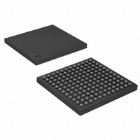
AT91SAM7L128-CU Atmel, AT91SAM7L128-CU Datasheet - Page 145

AT91SAM7L128-CU
Manufacturer Part Number
AT91SAM7L128-CU
Description
MCU ARM7 128K HS FLASH 144-LFBGA
Manufacturer
Atmel
Series
AT91SAMr
Datasheet
1.AT91SAM7L64-CU.pdf
(564 pages)
Specifications of AT91SAM7L128-CU
Core Processor
ARM7
Core Size
16/32-Bit
Speed
36MHz
Connectivity
I²C, SPI, UART/USART
Peripherals
Brown-out Detect/Reset, LCD, POR, PWM, WDT
Number Of I /o
80
Program Memory Size
128KB (128K x 8)
Program Memory Type
FLASH
Ram Size
6K x 8
Voltage - Supply (vcc/vdd)
1.55 V ~ 1.8 V
Data Converters
A/D 4x10b
Oscillator Type
Internal
Operating Temperature
-40°C ~ 85°C
Package / Case
144-LFBGA
Processor Series
AT91SAMx
Core
ARM7TDMI
Data Bus Width
32 bit
Data Ram Size
6 KB
Interface Type
2-Wire, SPI, USART
Maximum Clock Frequency
36 MHz
Number Of Programmable I/os
80
Number Of Timers
3
Maximum Operating Temperature
+ 85 C
Mounting Style
SMD/SMT
3rd Party Development Tools
JTRACE-ARM-2M, MDK-ARM, RL-ARM, ULINK2
Development Tools By Supplier
AT91SAM-ICE, AT91-ISP, AT91SAM7L-EK
Minimum Operating Temperature
- 40 C
On-chip Adc
10 bit, 4 Channel
For Use With
AT91SAM7L-STK - KIT EVAL FOR AT91SAM7LAT91SAM-ICE - EMULATOR FOR AT91 ARM7/ARM9
Lead Free Status / RoHS Status
Lead free / RoHS Compliant
Eeprom Size
-
Lead Free Status / Rohs Status
Details
Available stocks
Company
Part Number
Manufacturer
Quantity
Price
Company:
Part Number:
AT91SAM7L128-CU
Manufacturer:
Atmel
Quantity:
2 660
- Current page: 145 of 564
- Download datasheet (9Mb)
19.3.2.2
Figure 19-5. Data Read Optimization in ARM Mode for FWS = 1
19.3.3
6257A–ATARM–20-Feb-08
Buffer (128bits)
Flash Access
ARM Request
Data To ARM
Master Clock
(32-bit)
Flash Commands
Data Read Optimization
@Byte 0
XXX
XXX
XXX
The organization of the Flash in 128 bits is associated with two 128-bit prefetch buffers and one
128-bit data read buffer, thus providing maximum system performance. This buffer is added in
order to start access at the following data during the second read. This speeds up sequential
data reads if, for example, FWS is equal to 1 (see
Note:
The Enhanced Embedded Flash Controller (EEFC) offers a set of commands such as program-
ming the memory Flash, locking and unlocking lock regions, consecutive programming and
locking and full Flash erasing, etc.
Commands and read operations can be performed in parallel only on different memory planes.
Code can be fetched from one memory plane while a write or an erase operation is performed
on another.
Table 19-1.
Bytes 0-15
Command
Get Flash Descriptor
Write page
Write page and lock
Erase page and write page
Erase page and write page then lock
Erase all
Set Lock Bit
Clear Lock Bit
Get Lock Bit
Bytes 0-3
@ 4
No consecutive data read accesses are mandatory to benefit from this optimization.
Set of Commands
@ 8
4-7
@ 12
8-11
Bytes 0-15
12-15
@ 16
AT91SAM7L128/64 Preliminary
Bytes 16-31
@ 20
16-19
Figure
@ 24
20-23
19-5).
Value
0x0
0x1
0x2
0x3
0x4
0x5
0x8
0x9
0xA
24-27
@ 28
Bytes 16-31
28-31
@ 32
Mnemonic
GETD
WP
WPL
EWP
EWPL
EA
SLB
CLB
GLB
Bytes 32-47
@ 36
32-35
145
Related parts for AT91SAM7L128-CU
Image
Part Number
Description
Manufacturer
Datasheet
Request
R

Part Number:
Description:
KIT EVAL FOR AT91SAM7L
Manufacturer:
Atmel
Datasheet:

Part Number:
Description:
DEV KIT FOR AVR/AVR32
Manufacturer:
Atmel
Datasheet:

Part Number:
Description:
INTERVAL AND WIPE/WASH WIPER CONTROL IC WITH DELAY
Manufacturer:
ATMEL Corporation
Datasheet:

Part Number:
Description:
Low-Voltage Voice-Switched IC for Hands-Free Operation
Manufacturer:
ATMEL Corporation
Datasheet:

Part Number:
Description:
MONOLITHIC INTEGRATED FEATUREPHONE CIRCUIT
Manufacturer:
ATMEL Corporation
Datasheet:

Part Number:
Description:
AM-FM Receiver IC U4255BM-M
Manufacturer:
ATMEL Corporation
Datasheet:

Part Number:
Description:
Monolithic Integrated Feature Phone Circuit
Manufacturer:
ATMEL Corporation
Datasheet:

Part Number:
Description:
Multistandard Video-IF and Quasi Parallel Sound Processing
Manufacturer:
ATMEL Corporation
Datasheet:

Part Number:
Description:
High-performance EE PLD
Manufacturer:
ATMEL Corporation
Datasheet:

Part Number:
Description:
8-bit Flash Microcontroller
Manufacturer:
ATMEL Corporation
Datasheet:

Part Number:
Description:
2-Wire Serial EEPROM
Manufacturer:
ATMEL Corporation
Datasheet:


