AT91SAM7L128-CU Atmel, AT91SAM7L128-CU Datasheet - Page 473
AT91SAM7L128-CU
Manufacturer Part Number
AT91SAM7L128-CU
Description
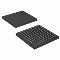
MCU ARM7 128K HS FLASH 144-LFBGA
Manufacturer
Atmel
Series
AT91SAMr
Datasheet
1.AT91SAM7L64-CU.pdf
(564 pages)
Specifications of AT91SAM7L128-CU
Core Processor
ARM7
Core Size
16/32-Bit
Speed
36MHz
Connectivity
I²C, SPI, UART/USART
Peripherals
Brown-out Detect/Reset, LCD, POR, PWM, WDT
Number Of I /o
80
Program Memory Size
128KB (128K x 8)
Program Memory Type
FLASH
Ram Size
6K x 8
Voltage - Supply (vcc/vdd)
1.55 V ~ 1.8 V
Data Converters
A/D 4x10b
Oscillator Type
Internal
Operating Temperature
-40°C ~ 85°C
Package / Case
144-LFBGA
Processor Series
AT91SAMx
Core
ARM7TDMI
Data Bus Width
32 bit
Data Ram Size
6 KB
Interface Type
2-Wire, SPI, USART
Maximum Clock Frequency
36 MHz
Number Of Programmable I/os
80
Number Of Timers
3
Maximum Operating Temperature
+ 85 C
Mounting Style
SMD/SMT
3rd Party Development Tools
JTRACE-ARM-2M, MDK-ARM, RL-ARM, ULINK2
Development Tools By Supplier
AT91SAM-ICE, AT91-ISP, AT91SAM7L-EK
Minimum Operating Temperature
- 40 C
On-chip Adc
10 bit, 4 Channel
For Use With
AT91SAM7L-STK - KIT EVAL FOR AT91SAM7LAT91SAM-ICE - EMULATOR FOR AT91 ARM7/ARM9
Lead Free Status / RoHS Status
Lead free / RoHS Compliant
Eeprom Size
-
Lead Free Status / Rohs Status
Details
Available stocks
Company
Part Number
Manufacturer
Quantity
Price
Company:

Part Number:
AT91SAM7L128-CU
Manufacturer:
Atmel
Quantity:
2 660


33. Analog-to-Digital Converter (ADC)
33.1
33.2
6257A–ATARM–20-Feb-08
Overview
Block Diagram
The ADC is based on a Successive Approximation Register (SAR) 10-bit Analog-to-Digital Con-
verter (ADC). It also integrates a 4-to-1 analog multiplexer, making possible the analog-to-digital
conversions of 4 analog lines. The conversions extend from 0V to ADVREF.
The ADC supports an 8-bit or 10-bit resolution mode, and conversion results are reported in a
common register for all channels, as well as in a channel-dedicated register. Software trigger,
external trigger on rising edge of the ADTRG pin or internal triggers from Timer Counter out-
put(s) are configurable.
The ADC also integrates a Sleep Mode and a conversion sequencer and connects with a PDC
channel. These features reduce both power consumption and processor intervention.
Finally, the user can configure ADC timings, such as Startup Time and Sample & Hold Time.
Figure 33-1. Analog-to-Digital Converter Block Diagram
Dedicated
Analog
Inputs
ADVREF
ADTRG
GND
AD-
AD-
AD-
Selection
Channels
Trigger
Counter
AT91SAM7L128/64 Preliminary
Timer
Analog-to-Digital
Approximation
Successive
Converter
Register
ADC
Interface
Control
Logic
User
ADC Interrupt
PDC
AIC
Peripheral Bridge
ASB
APB
473
Related parts for AT91SAM7L128-CU
Image
Part Number
Description
Manufacturer
Datasheet
Request
R

Part Number:
Description:
KIT EVAL FOR AT91SAM7L
Manufacturer:
Atmel
Datasheet:

Part Number:
Description:
DEV KIT FOR AVR/AVR32
Manufacturer:
Atmel
Datasheet:

Part Number:
Description:
INTERVAL AND WIPE/WASH WIPER CONTROL IC WITH DELAY
Manufacturer:
ATMEL Corporation
Datasheet:
Part Number:
Description:
Low-Voltage Voice-Switched IC for Hands-Free Operation
Manufacturer:
ATMEL Corporation
Datasheet:
Part Number:
Description:
MONOLITHIC INTEGRATED FEATUREPHONE CIRCUIT
Manufacturer:
ATMEL Corporation
Datasheet:
Part Number:
Description:
AM-FM Receiver IC U4255BM-M
Manufacturer:
ATMEL Corporation
Datasheet:
Part Number:
Description:
Monolithic Integrated Feature Phone Circuit
Manufacturer:
ATMEL Corporation
Datasheet:
Part Number:
Description:
Multistandard Video-IF and Quasi Parallel Sound Processing
Manufacturer:
ATMEL Corporation
Datasheet:
Part Number:
Description:
High-performance EE PLD
Manufacturer:
ATMEL Corporation
Datasheet:
Part Number:
Description:
8-bit Flash Microcontroller
Manufacturer:
ATMEL Corporation
Datasheet:
Part Number:
Description:
2-Wire Serial EEPROM
Manufacturer:
ATMEL Corporation
Datasheet: