AT91SAM7L128-CU Atmel, AT91SAM7L128-CU Datasheet - Page 163
AT91SAM7L128-CU
Manufacturer Part Number
AT91SAM7L128-CU
Description
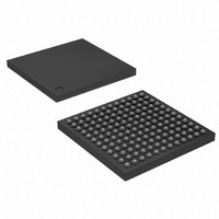
MCU ARM7 128K HS FLASH 144-LFBGA
Manufacturer
Atmel
Series
AT91SAMr
Datasheet
1.AT91SAM7L64-CU.pdf
(564 pages)
Specifications of AT91SAM7L128-CU
Core Processor
ARM7
Core Size
16/32-Bit
Speed
36MHz
Connectivity
I²C, SPI, UART/USART
Peripherals
Brown-out Detect/Reset, LCD, POR, PWM, WDT
Number Of I /o
80
Program Memory Size
128KB (128K x 8)
Program Memory Type
FLASH
Ram Size
6K x 8
Voltage - Supply (vcc/vdd)
1.55 V ~ 1.8 V
Data Converters
A/D 4x10b
Oscillator Type
Internal
Operating Temperature
-40°C ~ 85°C
Package / Case
144-LFBGA
Processor Series
AT91SAMx
Core
ARM7TDMI
Data Bus Width
32 bit
Data Ram Size
6 KB
Interface Type
2-Wire, SPI, USART
Maximum Clock Frequency
36 MHz
Number Of Programmable I/os
80
Number Of Timers
3
Maximum Operating Temperature
+ 85 C
Mounting Style
SMD/SMT
3rd Party Development Tools
JTRACE-ARM-2M, MDK-ARM, RL-ARM, ULINK2
Development Tools By Supplier
AT91SAM-ICE, AT91-ISP, AT91SAM7L-EK
Minimum Operating Temperature
- 40 C
On-chip Adc
10 bit, 4 Channel
For Use With
AT91SAM7L-STK - KIT EVAL FOR AT91SAM7LAT91SAM-ICE - EMULATOR FOR AT91 ARM7/ARM9
Lead Free Status / RoHS Status
Lead free / RoHS Compliant
Eeprom Size
-
Lead Free Status / Rohs Status
Details
Available stocks
Company
Part Number
Manufacturer
Quantity
Price
Company:

Part Number:
AT91SAM7L128-CU
Manufacturer:
Atmel
Quantity:
2 660


20.2.5.3
20.2.5.4
6257A–ATARM–20-Feb-08
Flash Full Erase Command
Flash Lock Commands
The Write Page command (WP) is optimized for consecutive writes. Write handshaking can be
chained; an internal address buffer is automatically increased.
Table 20-7.
The Flash command Write Page and Lock (WPL) is equivalent to the Flash Write Command.
However, the lock bit is automatically set at the end of the Flash write operation. As a lock region
is composed of several pages, the programmer writes to the first pages of the lock region using
Flash write commands and writes to the last page of the lock region using a Flash write and lock
command.
The Flash command Erase Page and Write (EWP) is equivalent to the Flash Write Command.
However, before programming the load buffer, the page is erased.
The Flash command Erase Page and Write the Lock (EWPL) combines EWP and WPL
commands.
This command is used to erase the Flash memory planes.
All lock regions must be unlocked before the Full Erase command by using the CLB command.
Otherwise, the erase command is aborted and no page is erased.
Table 20-8.
Lock bits can be set using WPL or EWPL commands. They can also be set by using the Set
Lock command (SLB). With this command, several lock bits can be activated. A Bit Mask is pro-
vided as argument to the command. When bit 0 of the bit mask is set, then the first lock bit is
activated.
Step
1
2
3
4
5
...
n
n+1
n+2
n+3
...
Step
1
2
Handshake Sequence
Write handshaking
Write handshaking
Write handshaking
Write handshaking
Write handshaking
...
Write handshaking
Write handshaking
Write handshaking
Write handshaking
...
Handshake Sequence
Write handshaking
Write handshaking
Write Command
Full Erase Command
AT91SAM7L128/64 Preliminary
ADDR1
...
ADDR1
DATA
DATA
...
MODE[3:0]
CMDE
ADDR0
DATA
DATA
ADDR0
MODE[3:0]
CMDE
DATA
DATA[15:0]
WP or WPL or EWP or EWPL
Memory Address LSB
Memory Address
*Memory Address++
*Memory Address++
...
Memory Address LSB
Memory Address
*Memory Address++
*Memory Address++
...
DATA[15:0]
EA
0
163
Related parts for AT91SAM7L128-CU
Image
Part Number
Description
Manufacturer
Datasheet
Request
R

Part Number:
Description:
KIT EVAL FOR AT91SAM7L
Manufacturer:
Atmel
Datasheet:

Part Number:
Description:
DEV KIT FOR AVR/AVR32
Manufacturer:
Atmel
Datasheet:

Part Number:
Description:
INTERVAL AND WIPE/WASH WIPER CONTROL IC WITH DELAY
Manufacturer:
ATMEL Corporation
Datasheet:
Part Number:
Description:
Low-Voltage Voice-Switched IC for Hands-Free Operation
Manufacturer:
ATMEL Corporation
Datasheet:
Part Number:
Description:
MONOLITHIC INTEGRATED FEATUREPHONE CIRCUIT
Manufacturer:
ATMEL Corporation
Datasheet:
Part Number:
Description:
AM-FM Receiver IC U4255BM-M
Manufacturer:
ATMEL Corporation
Datasheet:
Part Number:
Description:
Monolithic Integrated Feature Phone Circuit
Manufacturer:
ATMEL Corporation
Datasheet:
Part Number:
Description:
Multistandard Video-IF and Quasi Parallel Sound Processing
Manufacturer:
ATMEL Corporation
Datasheet:
Part Number:
Description:
High-performance EE PLD
Manufacturer:
ATMEL Corporation
Datasheet:
Part Number:
Description:
8-bit Flash Microcontroller
Manufacturer:
ATMEL Corporation
Datasheet:
Part Number:
Description:
2-Wire Serial EEPROM
Manufacturer:
ATMEL Corporation
Datasheet: