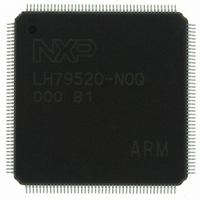
LH79520N0Q000B1;55 NXP Semiconductors, LH79520N0Q000B1;55 Datasheet - Page 24

LH79520N0Q000B1;55
Manufacturer Part Number
LH79520N0Q000B1;55
Description
IC ARM7 BLUESTREAK MCU 176LQFP
Manufacturer
NXP Semiconductors
Series
BlueStreak ; LH7r
Datasheet
1.LH79520N0Q000B155.pdf
(59 pages)
Specifications of LH79520N0Q000B1;55
Package / Case
176-LQFP
Core Processor
ARM7
Core Size
32-Bit
Speed
77.4MHz
Connectivity
EBI/EMI, IrDA, Microwire, SPI, SSI, SSP, UART/USART
Peripherals
DMA, LCD, POR, PWM, WDT
Number Of I /o
64
Program Memory Type
ROMless
Ram Size
32K x 8
Voltage - Supply (vcc/vdd)
1.62 V ~ 3.6 V
Oscillator Type
External
Operating Temperature
-40°C ~ 85°C
Processor Series
LH795
Core
ARM7TDMI-S
Data Bus Width
32 bit
Data Ram Size
32 KB
Interface Type
JTAG, UART
Maximum Clock Frequency
77.4 MHz
Number Of Programmable I/os
64
Number Of Timers
3
Operating Supply Voltage
1.8 V
Maximum Operating Temperature
+ 85 C
Mounting Style
SMD/SMT
3rd Party Development Tools
MDK-ARM, RL-ARM, ULINK2
Minimum Operating Temperature
- 40 C
Lead Free Status / RoHS Status
Lead free / RoHS Compliant
Eeprom Size
-
Program Memory Size
-
Data Converters
-
Lead Free Status / Rohs Status
Lead free / RoHS Compliant
Other names
568-4331
935285044557
LH79520N0Q000B1
935285044557
LH79520N0Q000B1
LH79520
AC Specifications
after a reference clock signal. The illustration in Figure
7 represents all cases of these sets of measurement
parameters; except for the Asynchronous Memory
Interface — which are referenced to Address Valid.
• HCLK, the System Bus clock
• PCLK, the Peripheral Bus clock (locked to HCLK in
• SSPCLK, the Synchronous Serial Interface clock
• UARTCLK, the UART Interface clock
• LCDDCLK, the LCD Data clock from the
• and SDCLK, the SDRAM clock.
point of the clock to the 50 % point of the signal. See
Figure 7.
24
the LH79520)
LCD Controller
All signals described in Table 8 relate to transitions
The reference clock signals in this design are:
All signal transitions are measured from the 50 %
REFERENCE
SIGNAL (O)
SIGNAL (I)
CLOCK
OUTPUT
INPUT
Figure 7. LH79520 Signal Timing
tOVXXX
Rev. 01 — 16 July 2007
NXP Semiconductors
represents the amount of time for the output to become
valid from the rising edge of the reference clock signal.
Maximum requirements for tOVXXX are shown in
Table 8.
amount of time the output will be held valid from the ris-
ing edge of the reference clock signal. Minimum
requirements for tOHXXX are listed in Table 8.
amount of time the input signal must be valid before the
rising edge of the clock signal. Minimum requirements
for tISXXX are shown in Table 8.
amount of time the memory output must be held valid
from the rising edge of the reference clock signal. Min-
imum requirements are shown in Table 8.
tISXXX tIHXXX
For outputs from the LH79520, tOVXXX (e.g. tOVA)
The signal tOHXXX (e.g. tOHA) represents the
For Inputs, tISXXX (e.g. tISD) represents the
The signal tIHXXX (e.g. tIHD) represents the
tOHXXX
Preliminary data sheet
System-on-Chip
79520-34


