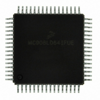
MC908LD64IFUE Freescale Semiconductor, MC908LD64IFUE Datasheet - Page 276

MC908LD64IFUE
Manufacturer Part Number
MC908LD64IFUE
Description
IC MCU 8BIT FOR LCD 64-QFP
Manufacturer
Freescale Semiconductor
Series
HC08r
Datasheet
1.MC908LD64IFUE.pdf
(362 pages)
Specifications of MC908LD64IFUE
Core Processor
HC08
Core Size
8-Bit
Speed
6MHz
Connectivity
I²C, USB
Peripherals
OSD, POR, PWM
Number Of I /o
39
Program Memory Size
60KB (60K x 8)
Program Memory Type
FLASH
Ram Size
2K x 8
Voltage - Supply (vcc/vdd)
3 V ~ 3.6 V
Data Converters
A/D 6x8b
Oscillator Type
Internal
Operating Temperature
0°C ~ 85°C
Package / Case
64-QFP
Processor Series
HC08LD
Core
HC08
Data Bus Width
8 bit
Data Ram Size
2 KB
Interface Type
I2C, USB
Maximum Clock Frequency
6 MHz
Number Of Programmable I/os
39
Number Of Timers
2
Maximum Operating Temperature
+ 85 C
Mounting Style
SMD/SMT
Development Tools By Supplier
FSICEBASE, M68CBL05CE
Minimum Operating Temperature
0 C
On-chip Adc
8 bit, 6 Channel
Lead Free Status / RoHS Status
Lead free / RoHS Compliant
Eeprom Size
-
Lead Free Status / Rohs Status
Details
Available stocks
Company
Part Number
Manufacturer
Quantity
Price
Company:
Part Number:
MC908LD64IFUE
Manufacturer:
Freescale Semiconductor
Quantity:
10 000
Part Number:
MC908LD64IFUE
Manufacturer:
FREESCALE
Quantity:
20 000
- Current page: 276 of 362
- Download datasheet (2Mb)
On-Screen Display (OSD)
18.6 OSD Screen Memory Map
Data Sheet
276
The OSD operating screen is mapped to a 1K-byte RAM array from
$0800 to $0BFF. The array is organized as 16 rows by 32 columns, with
two bytes (16-bit) for each row-column location.
OSD screen memory map.
The area covering row0-column0 and row14-column29 are called the
active display registers. Each 16-bit display register defines the
character to be displayed, with an character code (character from font
memory) and an attribute code for that character. Column30 of each row
is the attribute register for the entire row. Row15 registers (not memory
mapped) are used for control, window, and pattern for the entire OSD
screen. See
The CPU have direct access to the all screen memory registers ($0800
to $0BFF) when the OSDMEN bit in the OSD control register is clear.
When the OSD circuitry is displaying the characters (OSDMEN=1),
updates to display is by indirectly writing to these registers. The OSD
data registers, row register, column register are used for this purpose.
See
Row Address Register
Register
DISPLAY RAM
$8C0
$9C0
$A00
$A40
$A80
$AC0
$B00
$B40
$B80
$840
$880
$900
$940
$980
NOT MAPPED
ADDRESS
18.7.3 OSD Data Registers
–
–
–
–
–
–
–
–
–
–
–
–
–
–
$8BF
$9BF
$A3F
$A7F
$ABF
$AFF
$B3F
$B7F
$BBF
$87F
$8FF
$93F
$97F
$9FF
COLUMN
(OSDCAR).
Figure 18-4. Memory Map of OSD Registers
ROW
18.8 OSD Registers
On-Screen Display (OSD)
10
11
12
13
14
15
0
1
2
3
4
5
6
7
8
9
A = Character ATTRIBUTE
A
A
A
A
A
A
A
A
A
A
A
A
A
A
A
0
C
C
C
C
C
C
C
C
C
C
C
C
C
C
C
A
A
A
A
A
A
A
A
A
A
A
A
A
A
A
C O N T R O L , W I N D O W , A N D P A T T E R N R E G I S T E R S
1
(OSDRAR), and
C
C
C
C
C
C
C
C
C
C
C
C
C
C
C
A
A
A
A
A
A
A
A
A
A
A
A
A
A
A
R E G I S T E R S
2
C
C
C
C
C
C
C
C
C
C
C
C
C
C
C
D I S P L A Y
A
A
A
A
A
A
A
A
A
A
A
A
A
A
A
(OSDDRH:OSDDRL),
C = Character CODE
3
for register definitions.
C
C
C
C
C
C
C
C
C
C
C
C
C
C
C
18.7.5 OSD Column Address
MC68HC908LD64
Figure 18-4
A
A
A
A
A
A
A
A
A
A
A
A
A
A
A
Freescale Semiconductor
28
C
C
C
C
C
C
C
C
C
C
C
C
C
C
C
A
A
A
A
A
A
A
A
A
A
A
A
A
A
A
29
18.7.4 OSD
C
C
C
C
C
C
C
C
C
C
C
C
C
C
C
shows the
30
—
Rev. 3.0
31
Related parts for MC908LD64IFUE
Image
Part Number
Description
Manufacturer
Datasheet
Request
R
Part Number:
Description:
Manufacturer:
Freescale Semiconductor, Inc
Datasheet:
Part Number:
Description:
Manufacturer:
Freescale Semiconductor, Inc
Datasheet:
Part Number:
Description:
Manufacturer:
Freescale Semiconductor, Inc
Datasheet:
Part Number:
Description:
Manufacturer:
Freescale Semiconductor, Inc
Datasheet:
Part Number:
Description:
Manufacturer:
Freescale Semiconductor, Inc
Datasheet:
Part Number:
Description:
Manufacturer:
Freescale Semiconductor, Inc
Datasheet:
Part Number:
Description:
Manufacturer:
Freescale Semiconductor, Inc
Datasheet:
Part Number:
Description:
Manufacturer:
Freescale Semiconductor, Inc
Datasheet:
Part Number:
Description:
Manufacturer:
Freescale Semiconductor, Inc
Datasheet:
Part Number:
Description:
Manufacturer:
Freescale Semiconductor, Inc
Datasheet:
Part Number:
Description:
Manufacturer:
Freescale Semiconductor, Inc
Datasheet:
Part Number:
Description:
Manufacturer:
Freescale Semiconductor, Inc
Datasheet:
Part Number:
Description:
Manufacturer:
Freescale Semiconductor, Inc
Datasheet:
Part Number:
Description:
Manufacturer:
Freescale Semiconductor, Inc
Datasheet:
Part Number:
Description:
Manufacturer:
Freescale Semiconductor, Inc
Datasheet:


