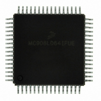
MC908LD64IFUE Freescale Semiconductor, MC908LD64IFUE Datasheet - Page 67

MC908LD64IFUE
Manufacturer Part Number
MC908LD64IFUE
Description
IC MCU 8BIT FOR LCD 64-QFP
Manufacturer
Freescale Semiconductor
Series
HC08r
Datasheet
1.MC908LD64IFUE.pdf
(362 pages)
Specifications of MC908LD64IFUE
Core Processor
HC08
Core Size
8-Bit
Speed
6MHz
Connectivity
I²C, USB
Peripherals
OSD, POR, PWM
Number Of I /o
39
Program Memory Size
60KB (60K x 8)
Program Memory Type
FLASH
Ram Size
2K x 8
Voltage - Supply (vcc/vdd)
3 V ~ 3.6 V
Data Converters
A/D 6x8b
Oscillator Type
Internal
Operating Temperature
0°C ~ 85°C
Package / Case
64-QFP
Processor Series
HC08LD
Core
HC08
Data Bus Width
8 bit
Data Ram Size
2 KB
Interface Type
I2C, USB
Maximum Clock Frequency
6 MHz
Number Of Programmable I/os
39
Number Of Timers
2
Maximum Operating Temperature
+ 85 C
Mounting Style
SMD/SMT
Development Tools By Supplier
FSICEBASE, M68CBL05CE
Minimum Operating Temperature
0 C
On-chip Adc
8 bit, 6 Channel
Lead Free Status / RoHS Status
Lead free / RoHS Compliant
Eeprom Size
-
Lead Free Status / Rohs Status
Details
Available stocks
Company
Part Number
Manufacturer
Quantity
Price
Company:
Part Number:
MC908LD64IFUE
Manufacturer:
Freescale Semiconductor
Quantity:
10 000
Part Number:
MC908LD64IFUE
Manufacturer:
FREESCALE
Quantity:
20 000
- Current page: 67 of 362
- Download datasheet (2Mb)
4.4.1 OSD FLASH Even High Byte Write Buffer (OSDEHBUF)
MC68HC908LD64
Freescale Semiconductor
—
Rev. 3.0
Figure 4-4. OSD FLASH Even High Byte Write Buffer (OSDEHBUF)
Address:
MASS — Mass Erase Control Bit
ERASE — Erase Control Bit
PGM — Program Control Bit
DOT[15:8] — OSD FLASH Even High Byte Buffer
These bits define the byte to be programmed to an even address
location of the 13K-bytes array. The contents of this register will be
automatically programmed to the even address ($xxxx) location when
the odd address ($xxxx+1) is programmed. Reset has no effect on these
bits. See
map.
Reset:
Read:
Write:
This read/write bit configures the memory for erase operation. ERASE
is interlocked with the PGM bit such that both bits cannot be equal to
1 or set to 1 at the same time.
This read/write bit configures the memory for mass erase operation or
block erase operation when the ERASE bit is set.
This read/write bit configures the memory for program operation.
PGM is interlocked with the ERASE bit such that both bits cannot be
equal to 1 or set to 1 at the same time.
1 = Mass Erase operation selected
0 = Mass Erase operation not selected
1 = Erase operation selected
0 = Erase operation not selected
1 = Program operation selected
0 = Program operation not selected
DOT15
$0066
Bit 7
18.5 OSD FLASH Font Memory Map
DOT14
FLASH Memory
6
DOT13
5
Unaffected by reset
DOT12
4
DOT11
3
for OSD font memory
DOT10
FLASH Control Registers
2
DOT9
FLASH Memory
1
Data Sheet
DOT8
0
67
Related parts for MC908LD64IFUE
Image
Part Number
Description
Manufacturer
Datasheet
Request
R
Part Number:
Description:
Manufacturer:
Freescale Semiconductor, Inc
Datasheet:
Part Number:
Description:
Manufacturer:
Freescale Semiconductor, Inc
Datasheet:
Part Number:
Description:
Manufacturer:
Freescale Semiconductor, Inc
Datasheet:
Part Number:
Description:
Manufacturer:
Freescale Semiconductor, Inc
Datasheet:
Part Number:
Description:
Manufacturer:
Freescale Semiconductor, Inc
Datasheet:
Part Number:
Description:
Manufacturer:
Freescale Semiconductor, Inc
Datasheet:
Part Number:
Description:
Manufacturer:
Freescale Semiconductor, Inc
Datasheet:
Part Number:
Description:
Manufacturer:
Freescale Semiconductor, Inc
Datasheet:
Part Number:
Description:
Manufacturer:
Freescale Semiconductor, Inc
Datasheet:
Part Number:
Description:
Manufacturer:
Freescale Semiconductor, Inc
Datasheet:
Part Number:
Description:
Manufacturer:
Freescale Semiconductor, Inc
Datasheet:
Part Number:
Description:
Manufacturer:
Freescale Semiconductor, Inc
Datasheet:
Part Number:
Description:
Manufacturer:
Freescale Semiconductor, Inc
Datasheet:
Part Number:
Description:
Manufacturer:
Freescale Semiconductor, Inc
Datasheet:
Part Number:
Description:
Manufacturer:
Freescale Semiconductor, Inc
Datasheet:


