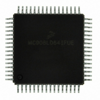
MC908LD64IFUE Freescale Semiconductor, MC908LD64IFUE Datasheet - Page 302

MC908LD64IFUE
Manufacturer Part Number
MC908LD64IFUE
Description
IC MCU 8BIT FOR LCD 64-QFP
Manufacturer
Freescale Semiconductor
Series
HC08r
Datasheet
1.MC908LD64IFUE.pdf
(362 pages)
Specifications of MC908LD64IFUE
Core Processor
HC08
Core Size
8-Bit
Speed
6MHz
Connectivity
I²C, USB
Peripherals
OSD, POR, PWM
Number Of I /o
39
Program Memory Size
60KB (60K x 8)
Program Memory Type
FLASH
Ram Size
2K x 8
Voltage - Supply (vcc/vdd)
3 V ~ 3.6 V
Data Converters
A/D 6x8b
Oscillator Type
Internal
Operating Temperature
0°C ~ 85°C
Package / Case
64-QFP
Processor Series
HC08LD
Core
HC08
Data Bus Width
8 bit
Data Ram Size
2 KB
Interface Type
I2C, USB
Maximum Clock Frequency
6 MHz
Number Of Programmable I/os
39
Number Of Timers
2
Maximum Operating Temperature
+ 85 C
Mounting Style
SMD/SMT
Development Tools By Supplier
FSICEBASE, M68CBL05CE
Minimum Operating Temperature
0 C
On-chip Adc
8 bit, 6 Channel
Lead Free Status / RoHS Status
Lead free / RoHS Compliant
Eeprom Size
-
Lead Free Status / Rohs Status
Details
Available stocks
Company
Part Number
Manufacturer
Quantity
Price
Company:
Part Number:
MC908LD64IFUE
Manufacturer:
Freescale Semiconductor
Quantity:
10 000
Part Number:
MC908LD64IFUE
Manufacturer:
FREESCALE
Quantity:
20 000
- Current page: 302 of 362
- Download datasheet (2Mb)
Input/Output (I/O) Ports
19.4.3 Port B Options
Data Sheet
302
Address:
When bit DDRBx is a logic 1, reading address $0001 reads the PTBx
data latch. When bit DDRBx is a logic 0, reading address $0001 reads
the voltage level on the pin. The data latch can always be written,
regardless of the state of its data direction bit.
the operation of the port B pins.
The PWM control register (PWMCR) selects the port B pins for PWM
function or as standard I/O function. (See
Modulator
PWM7E–PWM0E — PWM Output Enable Bits
Notes:
Reset:
1. X = don’t care.
2. Hi-Z = high impedance.
3. Writing affects data register, but does not affect input.
Read:
Write:
DDRB
Setting a PWMxE bit to logic 1 configures the PTBx/PWMx pin for
PWM output function. Reset clears the PWMxE bits.
Bit
0
1
1 = PTBx/PWMx pin configured as PWMx interrupt pin
0 = PTBx/PWMx pin configured as PTBx standard I/O pin
PWM7E
$0078
Bit 7
PTB Bit
0
Figure 19-9. PWM Control Register (PWMCR)
X
(PWM).)
X
(1)
Input/Output (I/O) Ports
PWM6E
6
0
Table 19-3. Port B Pin Functions
Input, Hi-Z
I/O Pin Mode
Output
PWM5E
5
0
(2)
Accesses to DDRB
PWM4E
4
0
DDRB[7:0]
DDRB[7:0]
Read/Write
PWM3E
Section 12. Pulse Width
3
0
Table 19-3
MC68HC908LD64
PWM2E
Freescale Semiconductor
PTB[7:0]
2
0
Read
Pin
Accesses to PTB
PWM1E
summarizes
1
0
PTB[7:0]
PTB[7:0]
—
Write
PWM0E
Rev. 3.0
Bit 0
0
(3)
Related parts for MC908LD64IFUE
Image
Part Number
Description
Manufacturer
Datasheet
Request
R
Part Number:
Description:
Manufacturer:
Freescale Semiconductor, Inc
Datasheet:
Part Number:
Description:
Manufacturer:
Freescale Semiconductor, Inc
Datasheet:
Part Number:
Description:
Manufacturer:
Freescale Semiconductor, Inc
Datasheet:
Part Number:
Description:
Manufacturer:
Freescale Semiconductor, Inc
Datasheet:
Part Number:
Description:
Manufacturer:
Freescale Semiconductor, Inc
Datasheet:
Part Number:
Description:
Manufacturer:
Freescale Semiconductor, Inc
Datasheet:
Part Number:
Description:
Manufacturer:
Freescale Semiconductor, Inc
Datasheet:
Part Number:
Description:
Manufacturer:
Freescale Semiconductor, Inc
Datasheet:
Part Number:
Description:
Manufacturer:
Freescale Semiconductor, Inc
Datasheet:
Part Number:
Description:
Manufacturer:
Freescale Semiconductor, Inc
Datasheet:
Part Number:
Description:
Manufacturer:
Freescale Semiconductor, Inc
Datasheet:
Part Number:
Description:
Manufacturer:
Freescale Semiconductor, Inc
Datasheet:
Part Number:
Description:
Manufacturer:
Freescale Semiconductor, Inc
Datasheet:
Part Number:
Description:
Manufacturer:
Freescale Semiconductor, Inc
Datasheet:
Part Number:
Description:
Manufacturer:
Freescale Semiconductor, Inc
Datasheet:


