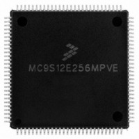
MC9S12E256MPVE Freescale Semiconductor, MC9S12E256MPVE Datasheet - Page 137

MC9S12E256MPVE
Manufacturer Part Number
MC9S12E256MPVE
Description
IC MCU 256K FLASH 25MHZ 112-LQFP
Manufacturer
Freescale Semiconductor
Series
HCS12r
Specifications of MC9S12E256MPVE
Core Processor
HCS12
Core Size
16-Bit
Speed
25MHz
Connectivity
EBI/EMI, I²C, SCI, SPI
Peripherals
POR, PWM, WDT
Number Of I /o
91
Program Memory Size
256KB (256K x 8)
Program Memory Type
FLASH
Ram Size
16K x 8
Voltage - Supply (vcc/vdd)
2.35 V ~ 2.75 V
Data Converters
A/D 16x10b; D/A 2x8b
Oscillator Type
Internal
Operating Temperature
-40°C ~ 125°C
Package / Case
112-LQFP
Processor Series
S12E
Core
HCS12
Data Bus Width
16 bit
Data Ram Size
16 KB
Interface Type
I2C/SCI/SPI
Maximum Clock Frequency
50 MHz
Number Of Programmable I/os
92
Number Of Timers
12
Operating Supply Voltage
0 V to 5 V
Maximum Operating Temperature
+ 125 C
Mounting Style
SMD/SMT
3rd Party Development Tools
EWHCS12
Minimum Operating Temperature
- 40 C
On-chip Adc
16-ch x 10-bit
On-chip Dac
2-ch x 8-bit
For Use With
M68EVB912E128 - BOARD EVAL FOR MC9S12E128/64
Lead Free Status / RoHS Status
Lead free / RoHS Compliant
Eeprom Size
-
Lead Free Status / Rohs Status
Lead free / RoHS Compliant
Available stocks
Company
Part Number
Manufacturer
Quantity
Price
Company:
Part Number:
MC9S12E256MPVE
Manufacturer:
Freescale Semiconductor
Quantity:
10 000
- Current page: 137 of 602
- Download datasheet (4Mb)
3.3.2.2
Read: Anytime. Write: Never, writes to this register have no effect.
This register always reads back the status of the associated pins.
3.3.2.3
Read: Anytime. Write: Anytime.
This register configures port pins PM[7:3] and PM[1:0] as either input or output.
If the IIC is enabled, the IIC controls the SCL and SDA I/O direction, and the corresponding DDRM[7:6]
bits have no effect on their I/O direction. Refer to
details.
If the SCI2 transmitter is enabled, the I/O direction of the transmit pin TXD2 is controlled by SCI2, and
the DDRM5 bit has no effect. If the SCI2 receiver is enabled, the I/O direction of the receive pin RXD2 is
controlled by SCI2, and the DDRM4 bit has no effect. Refer to
Interface (SCIV4)”
If the DAC1 or DAC0 channel is enabled, the associated pin DAO1 or DAO0 is forced to be output, and
the associated DDRM1 or DDRM0 bit has no effect.
The DDRM bits do not change to reflect the pin I/O direction when not being used as GPIO. The
DDRM[7:3]; DDRM[1:0] bits revert to controlling the I/O direction of the pins when the associated IIC,
SCI, or DAC1/0 function are disabled.
Freescale Semiconductor
DDRM[7:3,
7:3, 1:0
Reset
Reset
Field
1:0]
W
W
R
R
DDRM7
PTIM7
Data Direction Port M
0 Associated pin is configured as input.
1 Associated pin is configured as output.
Port M Input Register (PTIM)
Port M Data Direction Register (DDRM)
u
0
7
7
for further details.
= Reserved or Unimplemented
= Reserved or Unimplemented
DDRM6
PTIM6
u
0
6
6
Figure 3-12. Port M Data Direction Register (DDRM)
Figure 3-11. Port M Input Register (PTIM)
Table 3-9. DDRM Field Descriptions
DDRM5
PTIM5
MC9S12E256 Data Sheet, Rev. 1.08
u
0
5
5
DDRM4
PTIM4
u
0
Chapter 10, “Inter-Integrated Circuit (IICV2)”
4
4
Description
u = Unaffected by reset
DDRM3
PTIM3
3
u
3
0
Chapter 8, “Serial Communication
Chapter 3 Port Integration Module (PIM9E256V1)
0
0
0
0
2
2
DDRM1
PTIM1
u
0
1
1
DDRM0
PTIM0
for
u
0
0
0
137
Related parts for MC9S12E256MPVE
Image
Part Number
Description
Manufacturer
Datasheet
Request
R
Part Number:
Description:
Manufacturer:
Freescale Semiconductor, Inc
Datasheet:
Part Number:
Description:
Manufacturer:
Freescale Semiconductor, Inc
Datasheet:
Part Number:
Description:
Manufacturer:
Freescale Semiconductor, Inc
Datasheet:
Part Number:
Description:
Manufacturer:
Freescale Semiconductor, Inc
Datasheet:
Part Number:
Description:
Manufacturer:
Freescale Semiconductor, Inc
Datasheet:
Part Number:
Description:
Manufacturer:
Freescale Semiconductor, Inc
Datasheet:
Part Number:
Description:
Manufacturer:
Freescale Semiconductor, Inc
Datasheet:
Part Number:
Description:
Manufacturer:
Freescale Semiconductor, Inc
Datasheet:
Part Number:
Description:
Manufacturer:
Freescale Semiconductor, Inc
Datasheet:
Part Number:
Description:
Manufacturer:
Freescale Semiconductor, Inc
Datasheet:
Part Number:
Description:
Manufacturer:
Freescale Semiconductor, Inc
Datasheet:
Part Number:
Description:
Manufacturer:
Freescale Semiconductor, Inc
Datasheet:
Part Number:
Description:
Manufacturer:
Freescale Semiconductor, Inc
Datasheet:
Part Number:
Description:
Manufacturer:
Freescale Semiconductor, Inc
Datasheet:
Part Number:
Description:
Manufacturer:
Freescale Semiconductor, Inc
Datasheet:


