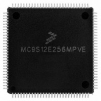
MC9S12E256MPVE Freescale Semiconductor, MC9S12E256MPVE Datasheet - Page 564

MC9S12E256MPVE
Manufacturer Part Number
MC9S12E256MPVE
Description
IC MCU 256K FLASH 25MHZ 112-LQFP
Manufacturer
Freescale Semiconductor
Series
HCS12r
Specifications of MC9S12E256MPVE
Core Processor
HCS12
Core Size
16-Bit
Speed
25MHz
Connectivity
EBI/EMI, I²C, SCI, SPI
Peripherals
POR, PWM, WDT
Number Of I /o
91
Program Memory Size
256KB (256K x 8)
Program Memory Type
FLASH
Ram Size
16K x 8
Voltage - Supply (vcc/vdd)
2.35 V ~ 2.75 V
Data Converters
A/D 16x10b; D/A 2x8b
Oscillator Type
Internal
Operating Temperature
-40°C ~ 125°C
Package / Case
112-LQFP
Processor Series
S12E
Core
HCS12
Data Bus Width
16 bit
Data Ram Size
16 KB
Interface Type
I2C/SCI/SPI
Maximum Clock Frequency
50 MHz
Number Of Programmable I/os
92
Number Of Timers
12
Operating Supply Voltage
0 V to 5 V
Maximum Operating Temperature
+ 125 C
Mounting Style
SMD/SMT
3rd Party Development Tools
EWHCS12
Minimum Operating Temperature
- 40 C
On-chip Adc
16-ch x 10-bit
On-chip Dac
2-ch x 8-bit
For Use With
M68EVB912E128 - BOARD EVAL FOR MC9S12E128/64
Lead Free Status / RoHS Status
Lead free / RoHS Compliant
Eeprom Size
-
Lead Free Status / Rohs Status
Lead free / RoHS Compliant
Available stocks
Company
Part Number
Manufacturer
Quantity
Price
Company:
Part Number:
MC9S12E256MPVE
Manufacturer:
Freescale Semiconductor
Quantity:
10 000
- Current page: 564 of 602
- Download datasheet (4Mb)
Appendix A Electrical Characteristics
A.1.7
This chapter describes the operating conditions of the device. Unless otherwise noted those conditions
apply to all the following data.
1
2
A.1.8
Power dissipation and thermal characteristics are closely related. The user must assure that the maximum
operating junction temperature is not exceeded. The average chip-junction temperature (T
obtained from:
The total power dissipation can be calculated from:
564
I/O, Regulator and Analog Supply Voltage
Internal Logic Supply Voltage
PLL Supply Voltage
Voltage Difference VDDX to VDDA
Voltage Difference VSSX to VSSR and VSSA
Oscillator
Bus Frequency
Operating Junction Temperature Range
The device contains an internal voltage regulator to generate the logic and PLL supply out of the I/O supply. The given
operating range applies when this regulator is disabled and the device is powered from an external source.
Some blocks e.g. ATD (conversion) and NVMs (program/erase) require higher bus frequencies for proper operation.
T
T
T
P
P
P
J
J
A
D
JA
D
INT
=
=
=
=
=
=
T
Junction Temperature, [ C
Ambient Temperature, [ C
Total Chip Power Dissipation, [W]
=
P
A
Package Thermal Resistance, [ C/W]
INT
Operating Conditions
Power Dissipation and Thermal Characteristics
Chip Internal Power Dissipation, [W]
+
2
Instead of specifying ambient temperature all parameters are specified for
the more meaningful silicon junction temperature. For power dissipation
calculations refer to
Characteristics”.
P
+
D
1
P
IO
JA
Rating
1
Section A.1.8, “Power Dissipation and Thermal
Table A-4. Operating Conditions
MC9S12E256 Data Sheet, Rev. 1.08
NOTE
Symbol
V
V
DDPLL
V
VDDX
VSSX
f
f
T
DD5
osc
bus
DD
J
2.97
2.35
2.35
–0.1
–0.1
0.25
Min
–40
0.5
3.3/5
Typ
2.5
2.5
—
—
—
0
0
Freescale Semiconductor
Max
2.75
2.75
140
J
5.5
0.1
0.1
16
25
) in C can be
MHz
MHz
Unit
V
V
V
V
V
C
Related parts for MC9S12E256MPVE
Image
Part Number
Description
Manufacturer
Datasheet
Request
R
Part Number:
Description:
Manufacturer:
Freescale Semiconductor, Inc
Datasheet:
Part Number:
Description:
Manufacturer:
Freescale Semiconductor, Inc
Datasheet:
Part Number:
Description:
Manufacturer:
Freescale Semiconductor, Inc
Datasheet:
Part Number:
Description:
Manufacturer:
Freescale Semiconductor, Inc
Datasheet:
Part Number:
Description:
Manufacturer:
Freescale Semiconductor, Inc
Datasheet:
Part Number:
Description:
Manufacturer:
Freescale Semiconductor, Inc
Datasheet:
Part Number:
Description:
Manufacturer:
Freescale Semiconductor, Inc
Datasheet:
Part Number:
Description:
Manufacturer:
Freescale Semiconductor, Inc
Datasheet:
Part Number:
Description:
Manufacturer:
Freescale Semiconductor, Inc
Datasheet:
Part Number:
Description:
Manufacturer:
Freescale Semiconductor, Inc
Datasheet:
Part Number:
Description:
Manufacturer:
Freescale Semiconductor, Inc
Datasheet:
Part Number:
Description:
Manufacturer:
Freescale Semiconductor, Inc
Datasheet:
Part Number:
Description:
Manufacturer:
Freescale Semiconductor, Inc
Datasheet:
Part Number:
Description:
Manufacturer:
Freescale Semiconductor, Inc
Datasheet:
Part Number:
Description:
Manufacturer:
Freescale Semiconductor, Inc
Datasheet:


