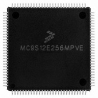
MC9S12E256MPVE Freescale Semiconductor, MC9S12E256MPVE Datasheet - Page 437

MC9S12E256MPVE
Manufacturer Part Number
MC9S12E256MPVE
Description
IC MCU 256K FLASH 25MHZ 112-LQFP
Manufacturer
Freescale Semiconductor
Series
HCS12r
Specifications of MC9S12E256MPVE
Core Processor
HCS12
Core Size
16-Bit
Speed
25MHz
Connectivity
EBI/EMI, I²C, SCI, SPI
Peripherals
POR, PWM, WDT
Number Of I /o
91
Program Memory Size
256KB (256K x 8)
Program Memory Type
FLASH
Ram Size
16K x 8
Voltage - Supply (vcc/vdd)
2.35 V ~ 2.75 V
Data Converters
A/D 16x10b; D/A 2x8b
Oscillator Type
Internal
Operating Temperature
-40°C ~ 125°C
Package / Case
112-LQFP
Processor Series
S12E
Core
HCS12
Data Bus Width
16 bit
Data Ram Size
16 KB
Interface Type
I2C/SCI/SPI
Maximum Clock Frequency
50 MHz
Number Of Programmable I/os
92
Number Of Timers
12
Operating Supply Voltage
0 V to 5 V
Maximum Operating Temperature
+ 125 C
Mounting Style
SMD/SMT
3rd Party Development Tools
EWHCS12
Minimum Operating Temperature
- 40 C
On-chip Adc
16-ch x 10-bit
On-chip Dac
2-ch x 8-bit
For Use With
M68EVB912E128 - BOARD EVAL FOR MC9S12E128/64
Lead Free Status / RoHS Status
Lead free / RoHS Compliant
Eeprom Size
-
Lead Free Status / Rohs Status
Lead free / RoHS Compliant
Available stocks
Company
Part Number
Manufacturer
Quantity
Price
Company:
Part Number:
MC9S12E256MPVE
Manufacturer:
Freescale Semiconductor
Quantity:
10 000
- Current page: 437 of 602
- Download datasheet (4Mb)
Chapter 14
Dual Output Voltage Regulator (VREG3V3V2)
14.1
The VREG is a dual output voltage regulator providing two separate 2.5 V (typical) supplies differing in
the amount of current that can be sourced. The regulator input voltage range is from 3.3 V up to 5 V
(typical).
14.1.1
The block VREG includes these distinctive features:
14.1.2
There are three modes VREG can operate in:
Freescale Semiconductor
•
•
•
•
•
•
•
Two parallel, linear voltage regulators
— Bandgap reference
Low-voltage detect (LVD) with low-voltage interrupt (LVI)
Power-on reset (POR)
Low-voltage reset (LVR)
Full-performance mode (FPM) (MCU is not in stop mode)
The regulator is active, providing the nominal supply voltage of 2.5 V with full current sourcing
capability at both outputs. Features LVD (low-voltage detect), LVR (low-voltage reset), and POR
(power-on reset) are available.
Reduced-power mode (RPM) (MCU is in stop mode)
The purpose is to reduce power consumption of the device. The output voltage may degrade to a
lower value than in full-performance mode, additionally the current sourcing capability is
substantially reduced. Only the POR is available in this mode, LVD and LVR are disabled.
Shutdown mode
Controlled by V
for connectivity of V
This mode is characterized by minimum power consumption. The regulator outputs are in a high
impedance state, only the POR feature is available, LVD and LVR are disabled.
This mode must be used to disable the chip internal regulator VREG, i.e., to bypass the VREG to
use external supplies.
Introduction
Features
Modes of Operation
REGEN
REGEN
(see
).
Chapter 1, “MC9S12E256 Device Overview (MC9S12E256DGV1)”
MC9S12E256 Data Sheet, Rev. 1.08
437
Related parts for MC9S12E256MPVE
Image
Part Number
Description
Manufacturer
Datasheet
Request
R
Part Number:
Description:
Manufacturer:
Freescale Semiconductor, Inc
Datasheet:
Part Number:
Description:
Manufacturer:
Freescale Semiconductor, Inc
Datasheet:
Part Number:
Description:
Manufacturer:
Freescale Semiconductor, Inc
Datasheet:
Part Number:
Description:
Manufacturer:
Freescale Semiconductor, Inc
Datasheet:
Part Number:
Description:
Manufacturer:
Freescale Semiconductor, Inc
Datasheet:
Part Number:
Description:
Manufacturer:
Freescale Semiconductor, Inc
Datasheet:
Part Number:
Description:
Manufacturer:
Freescale Semiconductor, Inc
Datasheet:
Part Number:
Description:
Manufacturer:
Freescale Semiconductor, Inc
Datasheet:
Part Number:
Description:
Manufacturer:
Freescale Semiconductor, Inc
Datasheet:
Part Number:
Description:
Manufacturer:
Freescale Semiconductor, Inc
Datasheet:
Part Number:
Description:
Manufacturer:
Freescale Semiconductor, Inc
Datasheet:
Part Number:
Description:
Manufacturer:
Freescale Semiconductor, Inc
Datasheet:
Part Number:
Description:
Manufacturer:
Freescale Semiconductor, Inc
Datasheet:
Part Number:
Description:
Manufacturer:
Freescale Semiconductor, Inc
Datasheet:
Part Number:
Description:
Manufacturer:
Freescale Semiconductor, Inc
Datasheet:


