MCF5485CVR200 Freescale Semiconductor, MCF5485CVR200 Datasheet - Page 2
MCF5485CVR200
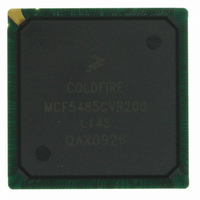
Manufacturer Part Number
MCF5485CVR200
Description
IC MPU 32BIT COLDF 388-PBGA
Manufacturer
Freescale Semiconductor
Series
MCF548xr
Datasheet
1.MCF5480CVR166.pdf
(34 pages)
Specifications of MCF5485CVR200
Core Processor
Coldfire V4E
Core Size
32-Bit
Speed
200MHz
Connectivity
CAN, EBI/EMI, Ethernet, I²C, SPI, UART/USART, USB
Peripherals
DMA, PWM, WDT
Number Of I /o
99
Program Memory Type
ROMless
Ram Size
32K x 8
Voltage - Supply (vcc/vdd)
1.43 V ~ 1.58 V
Oscillator Type
External
Operating Temperature
-40°C ~ 85°C
Package / Case
388-BGA
Processor Series
MCF548x
Core
ColdFire V4
Data Bus Width
32 bit
Data Ram Size
32 KB
Maximum Clock Frequency
83 MHz
Operating Supply Voltage
3 V to 3.6 V
Maximum Operating Temperature
+ 85 C
3rd Party Development Tools
JLINK-CF-BDM26, EWCF
Development Tools By Supplier
M5485EVBE, M5485EVBGHSE, M5484LITEKITE
Minimum Operating Temperature
- 40 C
Program Memory Size
64KB
Cpu Speed
200MHz
Embedded Interface Type
I2C, UART, DMA
Digital Ic Case Style
BGA
No. Of Pins
388
Rohs Compliant
Yes
For Use With
M5485EVBGHSE - KIT DEV GHS FOR M5485EVBM5485EVBGHS - KIT DEV GHS FOR M5485EVBM5485BFEE - MODULE MCF5485 FIRE ENGINEM5485AFEE - MODULE MCF5485 FIRE ENGINEM5485AFE - MODULE MCF5485 FIRE ENGINEM5484GFEE - MODULE M5484 FIRE ENGINEM5484LITEKITE - KIT DEV FOR MCF548X FAMILY
Lead Free Status / RoHS Status
Lead free / RoHS Compliant
Eeprom Size
-
Program Memory Size
-
Data Converters
-
Lead Free Status / Rohs Status
Lead free / RoHS Compliant
Available stocks
Company
Part Number
Manufacturer
Quantity
Price
Company:

Part Number:
MCF5485CVR200
Manufacturer:
FREESCAL
Quantity:
455
Company:
Part Number:
MCF5485CVR200
Manufacturer:
Freescale Semiconductor
Quantity:
10 000


1
2
3
4
5
6
7
8
9
10 PCI Bus. . . . . . . . . . . . . . . . . . . . . . . . . . . . . . . . . . . . . . . . . .21
11 Fast Ethernet AC Timing Specifications . . . . . . . . . . . . . . . . .22
12 General Timing Specifications . . . . . . . . . . . . . . . . . . . . . . . .25
13 I
14 JTAG and Boundary Scan Timing. . . . . . . . . . . . . . . . . . . . . .26
15 DSPI Electrical Specifications . . . . . . . . . . . . . . . . . . . . . . . .29
16 Timer Module AC Timing Specifications . . . . . . . . . . . . . . . . .29
17 Case Drawing . . . . . . . . . . . . . . . . . . . . . . . . . . . . . . . . . . . . .30
18 Revision History . . . . . . . . . . . . . . . . . . . . . . . . . . . . . . . . . . .32
List of Figures
2
Figure 1. MCF548X Block Diagram . . . . . . . . . . . . . . . . . . . . . . . 3
Figure 2. System PLL V
Figure 3. Supply Voltage Sequencing and Separation Cautions . 7
Figure 4. Preferred VBUS Connections . . . . . . . . . . . . . . . . . . . . 8
Figure 5. Alternate VBUS Connections . . . . . . . . . . . . . . . . . . . . 8
Figure 6. USB V
Figure 7. USBRBIAS Connection. . . . . . . . . . . . . . . . . . . . . . . . 10
Figure 8. Input Clock Timing Diagram . . . . . . . . . . . . . . . . . . . . 11
Figure 9. CLKIN, Internal Bus, and Core Clock Ratios . . . . . . . 11
Figure 10.Reset Timing . . . . . . . . . . . . . . . . . . . . . . . . . . . . . . . 12
Figure 11.FlexBus Read Timing . . . . . . . . . . . . . . . . . . . . . . . . 14
Figure 12.FlexBus Write Timing . . . . . . . . . . . . . . . . . . . . . . . . 15
Figure 13.SDR Write Timing . . . . . . . . . . . . . . . . . . . . . . . . . . . 17
Figure 14.SDR Read Timing . . . . . . . . . . . . . . . . . . . . . . . . . . . 17
Maximum Ratings . . . . . . . . . . . . . . . . . . . . . . . . . . . . . . . . . . .4
Thermal Characteristics . . . . . . . . . . . . . . . . . . . . . . . . . . . . . .4
2.1
2.2
DC Electrical Specifications . . . . . . . . . . . . . . . . . . . . . . . . . . .5
Hardware Design Considerations . . . . . . . . . . . . . . . . . . . . . . .6
4.1
4.2
4.3
4.4
Output Driver Capability and Loading. . . . . . . . . . . . . . . . . . .10
PLL Timing Specifications . . . . . . . . . . . . . . . . . . . . . . . . . . .11
Reset Timing Specifications . . . . . . . . . . . . . . . . . . . . . . . . . .12
FlexBus. . . . . . . . . . . . . . . . . . . . . . . . . . . . . . . . . . . . . . . . . .12
8.1
SDRAM Bus . . . . . . . . . . . . . . . . . . . . . . . . . . . . . . . . . . . . . .15
9.1
9.2
11.1 MII/7-WIRE Interface Timing Specs . . . . . . . . . . . . . . .22
11.2 MII Transmit Signal Timing . . . . . . . . . . . . . . . . . . . . . .23
11.3 MII Async Inputs Signal Timing (CRS, COL) . . . . . . . .24
11.4 MII Serial Management Channel Timing (MDIO,MDC).24
2
C Input/Output Timing Specifications. . . . . . . . . . . . . . . . . .25
Operating Temperatures . . . . . . . . . . . . . . . . . . . . . . . . .4
Thermal Resistance . . . . . . . . . . . . . . . . . . . . . . . . . . . .5
PLL Power Filtering. . . . . . . . . . . . . . . . . . . . . . . . . . . . .6
Supply Voltage Sequencing and Separation Cautions . .6
General USB Layout Guidelines . . . . . . . . . . . . . . . . . . .8
USB Power Filtering . . . . . . . . . . . . . . . . . . . . . . . . . . . .9
FlexBus AC Timing Characteristics. . . . . . . . . . . . . . . .13
SDR SDRAM AC Timing Characteristics . . . . . . . . . . .15
DDR SDRAM AC Timing Characteristics . . . . . . . . . . .18
DD
Power Filter . . . . . . . . . . . . . . . . . . . . . . . . . . 9
DD
Power Filter . . . . . . . . . . . . . . . . . . . . 6
MCF548x ColdFire
Table of Contents
®
Microprocessor, Rev. 4
List of Tables
Figure 15.DDR Clock Timing Diagram . . . . . . . . . . . . . . . . . . . . 18
Figure 16.DDR Write Timing . . . . . . . . . . . . . . . . . . . . . . . . . . . 20
Figure 17.DDR Read Timing . . . . . . . . . . . . . . . . . . . . . . . . . . . 21
Figure 18.PCI Timing . . . . . . . . . . . . . . . . . . . . . . . . . . . . . . . . . 22
Figure 19.MII Receive Signal Timing Diagram. . . . . . . . . . . . . . 23
Figure 20.MII Transmit Signal Timing Diagram . . . . . . . . . . . . . 23
Figure 21.MII Async Inputs Timing Diagram . . . . . . . . . . . . . . . 24
Figure 22.MII Serial Management Channel TIming Diagram. . . 24
Figure 23.I
Figure 24.Test Clock Input Timing . . . . . . . . . . . . . . . . . . . . . . . 27
Figure 25.Boundary Scan (JTAG) Timing . . . . . . . . . . . . . . . . . 27
Figure 26.Test Access Port Timing . . . . . . . . . . . . . . . . . . . . . . 27
Figure 27.TRST Timing Debug AC Timing Specifications . . . . . 27
Figure 28.Real-Time Trace AC Timing . . . . . . . . . . . . . . . . . . . . 28
Figure 29.BDM Serial Port AC Timing . . . . . . . . . . . . . . . . . . . . 28
Figure 30.DSPI Timing. . . . . . . . . . . . . . . . . . . . . . . . . . . . . . . . 29
Figure 31.388-pin BGA Case Outline. . . . . . . . . . . . . . . . . . . . . 31
Table 1. Absolute Maximum Ratings. . . . . . . . . . . . . . . . . . . . . . 4
Table 2. Operating Temperatures . . . . . . . . . . . . . . . . . . . . . . . . 4
Table 3. Thermal Resistance. . . . . . . . . . . . . . . . . . . . . . . . . . . . 5
Table 4. DC Electrical Specifications. . . . . . . . . . . . . . . . . . . . . . 5
Table 5. USB Filter Circuit Values . . . . . . . . . . . . . . . . . . . . . . . . 9
Table 6. I/O Driver Capability . . . . . . . . . . . . . . . . . . . . . . . . . . 10
Table 7. Clock Timing Specifications. . . . . . . . . . . . . . . . . . . . . 11
Table 8. MCF548x Divide Ratio Encodings. . . . . . . . . . . . . . . . 11
Table 9. Reset Timing Specifications . . . . . . . . . . . . . . . . . . . . 12
Table 10.FlexBus AC Timing Specifications. . . . . . . . . . . . . . . . 13
Table 11.SDR Timing Specifications . . . . . . . . . . . . . . . . . . . . . 16
Table 12.DDR Clock Crossover Specifications . . . . . . . . . . . . . 18
Table 13.DDR Timing Specifications . . . . . . . . . . . . . . . . . . . . . 18
Table 14.PCI Timing Specifications . . . . . . . . . . . . . . . . . . . . . . 21
Table 15.MII Receive Signal Timing . . . . . . . . . . . . . . . . . . . . . . 23
Table 16.MII Transmit Signal Timing . . . . . . . . . . . . . . . . . . . . . 23
Table 17.MII Transmit Signal Timing . . . . . . . . . . . . . . . . . . . . . 24
Table 18.MII Serial Management Channel Signal Timing . . . . . 24
Table 19.General AC Timing Specifications . . . . . . . . . . . . . . . . 25
Table 20.I
Table 21. I
Table 22.JTAG and Boundary Scan Timing . . . . . . . . . . . . . . . . 26
Table 23.Debug AC Timing Specifications . . . . . . . . . . . . . . . . . 28
Table 24.DSPI Modules AC Timing Specifications. . . . . . . . . . . 29
Table 25.Timer Module AC Timing Specifications . . . . . . . . . . . 29
SCL and SDA . . . . . . . . . . . . . . . . . . . . . . . . . . . . . . . 25
SCL and SDA . . . . . . . . . . . . . . . . . . . . . . . . . . . . . . . 25
2
2
C Input Timing Specifications between
2
C Output Timing Specifications between
C Input/Output Timings . . . . . . . . . . . . . . . . . . . . . . 26
Freescale Semiconductor
Related parts for MCF5485CVR200
Image
Part Number
Description
Manufacturer
Datasheet
Request
R

Part Number:
Description:
Integrated Microprocessor Electrical Characteristics
Manufacturer:
FREESCALE [Freescale Semiconductor, Inc]
Datasheet:

Part Number:
Description:
Manufacturer:
Freescale Semiconductor, Inc
Datasheet:
Part Number:
Description:
Manufacturer:
Freescale Semiconductor, Inc
Datasheet:
Part Number:
Description:
Manufacturer:
Freescale Semiconductor, Inc
Datasheet:
Part Number:
Description:
Manufacturer:
Freescale Semiconductor, Inc
Datasheet:
Part Number:
Description:
Manufacturer:
Freescale Semiconductor, Inc
Datasheet:
Part Number:
Description:
Manufacturer:
Freescale Semiconductor, Inc
Datasheet:
Part Number:
Description:
Manufacturer:
Freescale Semiconductor, Inc
Datasheet:
Part Number:
Description:
Manufacturer:
Freescale Semiconductor, Inc
Datasheet:
Part Number:
Description:
Manufacturer:
Freescale Semiconductor, Inc
Datasheet:
Part Number:
Description:
Manufacturer:
Freescale Semiconductor, Inc
Datasheet:
Part Number:
Description:
Manufacturer:
Freescale Semiconductor, Inc
Datasheet:
Part Number:
Description:
Manufacturer:
Freescale Semiconductor, Inc
Datasheet:
Part Number:
Description:
Manufacturer:
Freescale Semiconductor, Inc
Datasheet:
Part Number:
Description:
Manufacturer:
Freescale Semiconductor, Inc
Datasheet: