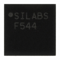
C8051F544-IM Silicon Laboratories Inc, C8051F544-IM Datasheet - Page 187

C8051F544-IM
Manufacturer Part Number
C8051F544-IM
Description
IC 8051 MCU 8K FLASH 32-QFN
Manufacturer
Silicon Laboratories Inc
Series
C8051F54xr
Specifications of C8051F544-IM
Program Memory Type
FLASH
Program Memory Size
8KB (8K x 8)
Package / Case
32-QFN
Mfg Application Notes
LIN Bootloader AppNote
Core Processor
8051
Core Size
8-Bit
Speed
50MHz
Connectivity
SMBus (2-Wire/I²C), LIN, SPI, UART/USART
Peripherals
POR, PWM, Temp Sensor, WDT
Number Of I /o
25
Ram Size
1.25K x 8
Voltage - Supply (vcc/vdd)
1.8 V ~ 5.25 V
Data Converters
A/D 25x12b
Oscillator Type
Internal
Operating Temperature
-40°C ~ 125°C
Processor Series
C8051F5x
Core
8051
Data Bus Width
8 bit
Data Ram Size
256 B
Maximum Clock Frequency
50 MHz
Number Of Programmable I/os
25
Operating Supply Voltage
1.8 V to 5.25 V
Maximum Operating Temperature
+ 125 C
Mounting Style
SMD/SMT
3rd Party Development Tools
PK51, CA51, A51, ULINK2
Development Tools By Supplier
C8051F540DK
Minimum Operating Temperature
- 40 C
Lead Free Status / RoHS Status
Lead free / RoHS Compliant
For Use With
336-1672 - BOARD PROTOTYPE W/C8051F540336-1669 - KIT DEVELOPMENT FOR C8051F540
Eeprom Size
-
Lead Free Status / Rohs Status
Lead free / RoHS Compliant
Other names
336-1677-5
Available stocks
Company
Part Number
Manufacturer
Quantity
Price
Company:
Part Number:
C8051F544-IM
Manufacturer:
Silicon Labs
Quantity:
135
- Current page: 187 of 274
- Download datasheet (3Mb)
20. SMBus
The SMBus I/O interface is a two-wire, bi-directional serial bus. The SMBus is compliant with the System
Management Bus Specification, version 1.1, and compatible with the I2C serial bus. Reads and writes to
the interface by the system controller are byte oriented with the SMBus interface autonomously controlling
the serial transfer of the data. Data can be transferred at up to 1/20th of the system clock as a master or
slave (this can be faster than allowed by the SMBus specification, depending on the system clock used). A
method of extending the clock-low duration is available to accommodate devices with different speed
capabilities on the same bus.
The SMBus interface may operate as a master and/or slave, and may function on a bus with multiple mas-
ters. The SMBus provides control of SDA (serial data), SCL (serial clock) generation and synchronization,
arbitration logic, and START/STOP control and generation. A block diagram of the SMBus peripheral and
the associated SFRs is shown in Figure 20.1.
M
A
S
T
E
R
Interrupt
Request
M
O
D
T
X
E
SMB0CN
S
T
A
S
O
T
Q
A
C
K
R
A
R
B
O
S
L
T
C
A
K
S
I
Arbitration
SCL Synchronization
SCL Generation (Master Mode)
SDA Control
IRQ Generation
SMBUS CONTROL LOGIC
M
E
N
S
B
Figure 20.1. SMBus Block Diagram
N
H
I
SMB0CF
B
U
S
Y
E
X
H
O
D
T
L
M
O
S
B
T
E
M
S
B
F
T
E
M
C
S
B
S
1
7
M
S
B
C
S
0
6
Data Path
SMB0DAT
5
Control
4
3
Rev. 1.1
2
1
0
00
01
10
11
Control
SDA
Control
SCL
T0 Overflow
T1 Overflow
TMR2H Overflow
TMR2L Overflow
FILTER
FILTER
N
N
SDA
SCL
C
R
O
S
S
B
A
R
C8051F54x
Port I/O
187
Related parts for C8051F544-IM
Image
Part Number
Description
Manufacturer
Datasheet
Request
R
Part Number:
Description:
SMD/C°/SINGLE-ENDED OUTPUT SILICON OSCILLATOR
Manufacturer:
Silicon Laboratories Inc
Part Number:
Description:
Manufacturer:
Silicon Laboratories Inc
Datasheet:
Part Number:
Description:
N/A N/A/SI4010 AES KEYFOB DEMO WITH LCD RX
Manufacturer:
Silicon Laboratories Inc
Datasheet:
Part Number:
Description:
N/A N/A/SI4010 SIMPLIFIED KEY FOB DEMO WITH LED RX
Manufacturer:
Silicon Laboratories Inc
Datasheet:
Part Number:
Description:
N/A/-40 TO 85 OC/EZLINK MODULE; F930/4432 HIGH BAND (REV E/B1)
Manufacturer:
Silicon Laboratories Inc
Part Number:
Description:
EZLink Module; F930/4432 Low Band (rev e/B1)
Manufacturer:
Silicon Laboratories Inc
Part Number:
Description:
I°/4460 10 DBM RADIO TEST CARD 434 MHZ
Manufacturer:
Silicon Laboratories Inc
Part Number:
Description:
I°/4461 14 DBM RADIO TEST CARD 868 MHZ
Manufacturer:
Silicon Laboratories Inc
Part Number:
Description:
I°/4463 20 DBM RFSWITCH RADIO TEST CARD 460 MHZ
Manufacturer:
Silicon Laboratories Inc
Part Number:
Description:
I°/4463 20 DBM RADIO TEST CARD 868 MHZ
Manufacturer:
Silicon Laboratories Inc
Part Number:
Description:
I°/4463 27 DBM RADIO TEST CARD 868 MHZ
Manufacturer:
Silicon Laboratories Inc
Part Number:
Description:
I°/4463 SKYWORKS 30 DBM RADIO TEST CARD 915 MHZ
Manufacturer:
Silicon Laboratories Inc
Part Number:
Description:
N/A N/A/-40 TO 85 OC/4463 RFMD 30 DBM RADIO TEST CARD 915 MHZ
Manufacturer:
Silicon Laboratories Inc
Part Number:
Description:
I°/4463 20 DBM RADIO TEST CARD 169 MHZ
Manufacturer:
Silicon Laboratories Inc


