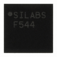
C8051F544-IM Silicon Laboratories Inc, C8051F544-IM Datasheet - Page 80

C8051F544-IM
Manufacturer Part Number
C8051F544-IM
Description
IC 8051 MCU 8K FLASH 32-QFN
Manufacturer
Silicon Laboratories Inc
Series
C8051F54xr
Specifications of C8051F544-IM
Program Memory Type
FLASH
Program Memory Size
8KB (8K x 8)
Package / Case
32-QFN
Mfg Application Notes
LIN Bootloader AppNote
Core Processor
8051
Core Size
8-Bit
Speed
50MHz
Connectivity
SMBus (2-Wire/I²C), LIN, SPI, UART/USART
Peripherals
POR, PWM, Temp Sensor, WDT
Number Of I /o
25
Ram Size
1.25K x 8
Voltage - Supply (vcc/vdd)
1.8 V ~ 5.25 V
Data Converters
A/D 25x12b
Oscillator Type
Internal
Operating Temperature
-40°C ~ 125°C
Processor Series
C8051F5x
Core
8051
Data Bus Width
8 bit
Data Ram Size
256 B
Maximum Clock Frequency
50 MHz
Number Of Programmable I/os
25
Operating Supply Voltage
1.8 V to 5.25 V
Maximum Operating Temperature
+ 125 C
Mounting Style
SMD/SMT
3rd Party Development Tools
PK51, CA51, A51, ULINK2
Development Tools By Supplier
C8051F540DK
Minimum Operating Temperature
- 40 C
Lead Free Status / RoHS Status
Lead free / RoHS Compliant
For Use With
336-1672 - BOARD PROTOTYPE W/C8051F540336-1669 - KIT DEVELOPMENT FOR C8051F540
Eeprom Size
-
Lead Free Status / Rohs Status
Lead free / RoHS Compliant
Other names
336-1677-5
Available stocks
Company
Part Number
Manufacturer
Quantity
Price
Company:
Part Number:
C8051F544-IM
Manufacturer:
Silicon Labs
Quantity:
135
- Current page: 80 of 274
- Download datasheet (3Mb)
C8051F54x
10.3. CIP-51 Register Descriptions
Following are descriptions of SFRs related to the operation of the CIP-51 System Controller. Reserved bits
should not be set to logic l. Future product versions may use these bits to implement new features in which
case the reset value of the bit will be logic 0, selecting the feature's default state. Detailed descriptions of
the remaining SFRs are included in the sections of the datasheet associated with their corresponding sys-
tem function.
80
Notes on Registers, Operands and Addressing Modes:
Rn—Register R0–R7 of the currently selected register bank.
@Ri—Data RAM location addressed indirectly through R0 or R1.
rel—8-bit, signed (two’s complement) offset relative to the first byte of the following instruction. Used by
SJMP and all conditional jumps.
direct—8-bit internal data location’s address. This could be a direct-access Data RAM location (0x00–
0x7F) or an SFR (0x80–0xFF).
#data—8-bit constant
#data16—16-bit constant
bit—Direct-accessed bit in Data RAM or SFR
addr11—11-bit destination address used by ACALL and AJMP. The destination must be within the
same 2 kB page of program memory as the first byte of the following instruction.
addr16—16-bit destination address used by LCALL and LJMP. The destination may be anywhere within
the 64 kB program memory space.
There is one unused opcode (0xA5) that performs the same function as NOP.
All mnemonics copyrighted © Intel Corporation 1980.
Rev. 1.1
Related parts for C8051F544-IM
Image
Part Number
Description
Manufacturer
Datasheet
Request
R
Part Number:
Description:
SMD/C°/SINGLE-ENDED OUTPUT SILICON OSCILLATOR
Manufacturer:
Silicon Laboratories Inc
Part Number:
Description:
Manufacturer:
Silicon Laboratories Inc
Datasheet:
Part Number:
Description:
N/A N/A/SI4010 AES KEYFOB DEMO WITH LCD RX
Manufacturer:
Silicon Laboratories Inc
Datasheet:
Part Number:
Description:
N/A N/A/SI4010 SIMPLIFIED KEY FOB DEMO WITH LED RX
Manufacturer:
Silicon Laboratories Inc
Datasheet:
Part Number:
Description:
N/A/-40 TO 85 OC/EZLINK MODULE; F930/4432 HIGH BAND (REV E/B1)
Manufacturer:
Silicon Laboratories Inc
Part Number:
Description:
EZLink Module; F930/4432 Low Band (rev e/B1)
Manufacturer:
Silicon Laboratories Inc
Part Number:
Description:
I°/4460 10 DBM RADIO TEST CARD 434 MHZ
Manufacturer:
Silicon Laboratories Inc
Part Number:
Description:
I°/4461 14 DBM RADIO TEST CARD 868 MHZ
Manufacturer:
Silicon Laboratories Inc
Part Number:
Description:
I°/4463 20 DBM RFSWITCH RADIO TEST CARD 460 MHZ
Manufacturer:
Silicon Laboratories Inc
Part Number:
Description:
I°/4463 20 DBM RADIO TEST CARD 868 MHZ
Manufacturer:
Silicon Laboratories Inc
Part Number:
Description:
I°/4463 27 DBM RADIO TEST CARD 868 MHZ
Manufacturer:
Silicon Laboratories Inc
Part Number:
Description:
I°/4463 SKYWORKS 30 DBM RADIO TEST CARD 915 MHZ
Manufacturer:
Silicon Laboratories Inc
Part Number:
Description:
N/A N/A/-40 TO 85 OC/4463 RFMD 30 DBM RADIO TEST CARD 915 MHZ
Manufacturer:
Silicon Laboratories Inc
Part Number:
Description:
I°/4463 20 DBM RADIO TEST CARD 169 MHZ
Manufacturer:
Silicon Laboratories Inc


