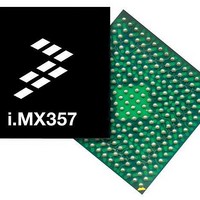
MCIMX357CJQ5C Freescale Semiconductor, MCIMX357CJQ5C Datasheet - Page 103

MCIMX357CJQ5C
Manufacturer Part Number
MCIMX357CJQ5C
Description
MPU MX35 ARM11 400-MAPBGA
Manufacturer
Freescale Semiconductor
Series
i.MX35r
Specifications of MCIMX357CJQ5C
Core Processor
ARM11
Core Size
32-Bit
Speed
532MHz
Connectivity
1-Wire, CAN, EBI/EMI, Ethernet, I²C, MMC, SPI, SSI, UART/USART, USB OTG
Peripherals
DMA, I²S, LCD, POR, PWM, WDT
Number Of I /o
96
Program Memory Type
ROMless
Ram Size
128K x 8
Voltage - Supply (vcc/vdd)
1.33 V ~ 1.47 V
Oscillator Type
External
Operating Temperature
-40°C ~ 85°C
Package / Case
400-MAPBGA
Processor Series
i.MX357
Core
ARM1136JF-S
Data Bus Width
32 bit
Data Ram Size
128 KB
Interface Type
I2C, JTAG, UART
Maximum Clock Frequency
532 MHz
Number Of Timers
3
Operating Supply Voltage
1.33 V to 1.47 V
Maximum Operating Temperature
+ 85 C
Mounting Style
SMD/SMT
Minimum Operating Temperature
- 40 C
Lead Free Status / RoHS Status
Lead free / RoHS Compliant
Eeprom Size
-
Program Memory Size
-
Data Converters
-
Lead Free Status / Rohs Status
Details
Available stocks
Company
Part Number
Manufacturer
Quantity
Price
Company:
Part Number:
MCIMX357CJQ5C
Manufacturer:
Freescale Semiconductor
Quantity:
10 000
Company:
Part Number:
MCIMX357CJQ5CR2
Manufacturer:
Freescale Semiconductor
Quantity:
10 000
Figure 77
Freescale Semiconductor
Parameter
ATA
tA
—
—
t1
t2
t9
t3
t4
t0
shows timing for PIO write, and
Parameter
Figure 77
from
t2w
—
—
—
—
t1
t9
t4
tA
i.MX35 Applications Processors for Industrial and Consumer Products, Rev. 9
t1 (min.) = time_1 × T – (tskew1 + tskew2 + tskew5)
t2 (min.) = time_2w × T – (tskew1 + tskew2 + tskew5)
t3 (min.) = (time_2w – time_on) × T – (tskew1 + tskew2 +tskew5)
t4 (min.) = time_4 × T – tskew1
tA = (1.5 + time_ax) × T – (tco + tsui + tcable2 + tcable2 + 2*tbuf)
t0(min.) = (time_1 + time_2 + time_9) × T
Avoid bus contention when switching buffer on by making ton long enough.
Avoid bus contention when switching buffer off by making toff long enough.
t9 (min.) = time_9 × T – (tskew1 + tskew2 + tskew6)
Table 67. PIO Write Timing Parameters
Figure 77. PIO Write Timing Diagram
Table 67
lists the timing parameters for PIO write.
Value
If not met, increase
time_1, time_2r,
Controlling
Variable
time_2w
time_2w
time_ax
time_9
time_4
time_9
time_1
—
—
103


