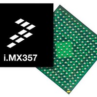
MCIMX357CJQ5C Freescale Semiconductor, MCIMX357CJQ5C Datasheet - Page 19

MCIMX357CJQ5C
Manufacturer Part Number
MCIMX357CJQ5C
Description
MPU MX35 ARM11 400-MAPBGA
Manufacturer
Freescale Semiconductor
Series
i.MX35r
Specifications of MCIMX357CJQ5C
Core Processor
ARM11
Core Size
32-Bit
Speed
532MHz
Connectivity
1-Wire, CAN, EBI/EMI, Ethernet, I²C, MMC, SPI, SSI, UART/USART, USB OTG
Peripherals
DMA, I²S, LCD, POR, PWM, WDT
Number Of I /o
96
Program Memory Type
ROMless
Ram Size
128K x 8
Voltage - Supply (vcc/vdd)
1.33 V ~ 1.47 V
Oscillator Type
External
Operating Temperature
-40°C ~ 85°C
Package / Case
400-MAPBGA
Processor Series
i.MX357
Core
ARM1136JF-S
Data Bus Width
32 bit
Data Ram Size
128 KB
Interface Type
I2C, JTAG, UART
Maximum Clock Frequency
532 MHz
Number Of Timers
3
Operating Supply Voltage
1.33 V to 1.47 V
Maximum Operating Temperature
+ 85 C
Mounting Style
SMD/SMT
Minimum Operating Temperature
- 40 C
Lead Free Status / RoHS Status
Lead free / RoHS Compliant
Eeprom Size
-
Program Memory Size
-
Data Converters
-
Lead Free Status / Rohs Status
Details
Available stocks
Company
Part Number
Manufacturer
Quantity
Price
Company:
Part Number:
MCIMX357CJQ5C
Manufacturer:
Freescale Semiconductor
Quantity:
10 000
Company:
Part Number:
MCIMX357CJQ5CR2
Manufacturer:
Freescale Semiconductor
Quantity:
10 000
532 MHz. Common supplies have been bundled according to the i.MX35 power-up sequence
requirements. Peak numbers are provided for system designers so that the i.MX35 power supply
requirements will be satisfied during startup and transient conditions. Freescale recommends that system
current measurements be taken with customer-specific use-cases to reflect normal operating conditions in
the end system.
1
The method for obtaining max current is as follows:
4.6
The thermal resistance characteristics for the device are given in
under the following conditions:
Freescale Semiconductor
QVCC
MVDD, PVDD
NVCC_EMI1, NVCC_EMI2, NVCC_EMI3, NVCC_LCDC, NVCC_NFC
FUSE_VDD
NVCC_MISC, NVCC_CSI, NVCC_SDIO, NVCC_CRM, NVCC_ATA, NVCC_MLB,
NVCC_JTAG
OSC24M_VDD, OSC_AUDIO_VDD, PHY1_VDDA, PHY2_VDD,
USBPHY1_UPLLVDD, USBPHY1_VDDA_BIAS
This rail is connected to ground; it only needs a voltage if eFuses are to be programmed. FUSE_VDD should be supplied by
following the power up sequence given in
1. Measure worst case power consumption on individual rails using directed test on i.MX35.
2. Correlate worst case power consumption power measurements with worst case power
3. Combine common voltage rails based on power supply sequencing requirements
4. Guard band worst case numbers for temperature and process variation. Guard band is based on
5. The sum of individual rails is greater than real world power consumption, as a real system does
•
•
•
•
•
•
•
•
consumption simulations.
process data and correlated with actual data measured on i.MX35.
not typically maximize power consumption on all peripherals simultaneously.
Two-layer substrate
Substrate solder mask thickness: 0.025 mm
Substrate metal thicknesses: 0.016 mm
Substrate core thickness: 0.200 mm
Core via I.D: 0.168 mm, Core via plating 0.016 mm.
Full array map design, but nearly all balls under die are power or ground.
Die Attach: 0.033 mm non-conductive die attach, k = 0.3 W/m K
Mold compound: k = 0.9 W/m K
Thermal Characteristics
1
i.MX35 Applications Processors for Industrial and Consumer Products, Rev. 9
Power Supply
Section 4.3.1, “Powering Up.”
Table 11. Power Consumption
Table
12. These values were measured
Voltage (V)
1.47
1.65
1.9
3.6
3.6
3.6
Max Current (mA)
400
20
90
62
60
25
19


