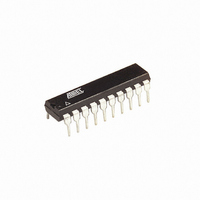
ATTINY26L-8PU Atmel, ATTINY26L-8PU Datasheet - Page 39

ATTINY26L-8PU
Manufacturer Part Number
ATTINY26L-8PU
Description
IC MCU AVR 2K 5V 8MHZ 20-DIP
Manufacturer
Atmel
Series
AVR® ATtinyr
Datasheets
1.ATTINY26-16MC.pdf
(18 pages)
2.ATTINY26-16MC.pdf
(182 pages)
3.ATTINY26L-8PU.pdf
(183 pages)
Specifications of ATTINY26L-8PU
Core Processor
AVR
Core Size
8-Bit
Speed
8MHz
Connectivity
USI
Peripherals
Brown-out Detect/Reset, POR, PWM, WDT
Number Of I /o
16
Program Memory Size
2KB (1K x 16)
Program Memory Type
FLASH
Eeprom Size
128 x 8
Ram Size
128 x 8
Voltage - Supply (vcc/vdd)
2.7 V ~ 5.5 V
Data Converters
A/D 11x10b
Oscillator Type
Internal
Operating Temperature
-40°C ~ 85°C
Package / Case
20-DIP (0.300", 7.62mm)
Processor Series
ATTINY2x
Core
AVR8
Data Bus Width
8 bit
Data Ram Size
128 B
Interface Type
2-Wire/ISP/SM-Bus/SPI/UART/USI
Maximum Clock Frequency
8 MHz
Number Of Programmable I/os
16
Number Of Timers
2
Operating Supply Voltage
2.7 V to 5.5 V
Maximum Operating Temperature
+ 85 C
Mounting Style
Through Hole
3rd Party Development Tools
EWAVR, EWAVR-BL
Development Tools By Supplier
ATAVRDRAGON, ATSTK500, ATSTK600, ATAVRISP2, ATAVRONEKIT
Minimum Operating Temperature
- 40 C
On-chip Adc
11-ch x 10-bit
Controller Family/series
AVR Tiny
No. Of I/o's
16
Eeprom Memory Size
128Byte
Ram Memory Size
128Byte
Cpu Speed
8MHz
Rohs Compliant
Yes
For Use With
ATSTK600 - DEV KIT FOR AVR/AVR32770-1007 - ISP 4PORT ATMEL AVR MCU SPI/JTAGATAVRISP2 - PROGRAMMER AVR IN SYSTEMATSTK505 - ADAPTER KIT FOR 14PIN AVR MCU
Lead Free Status / RoHS Status
Lead free / RoHS Compliant
Other names
ATTINY26L-8PJ
ATTINY26L-8PJ
ATTINY26L-8PJ
Available stocks
Company
Part Number
Manufacturer
Quantity
Price
Company:
Part Number:
ATTINY26L-8PU
Manufacturer:
Atmel
Quantity:
25 295
Part Number:
ATTINY26L-8PU
Manufacturer:
ATMEL/爱特梅尔
Quantity:
20 000
Minimizing Power
Consumption
Analog to Digital Converter
Analog Comparator
Brown-out Detector
Internal Voltage Reference
Watchdog Timer
Port Pins
1477F–AVR–12/04
There are several issues to consider when trying to minimize the power consumption in
an AVR controlled system. In general, sleep modes should be used as much as possi-
ble, and the sleep mode should be selected so that as few as possible of the device’s
functions are operating. All functions not needed should be disabled. In particular, the
following modules may need special consideration when trying to achieve the lowest
possible power consumption.
If enabled, the ADC will be enabled in all sleep modes. To save power, the ADC should
be disabled before entering any sleep mode. When the ADC is turned off and on again,
the next conversion will be an extended conversion. Refer to “Analog to Digital Con-
verter” on page 94 for details on ADC operation.
When entering Idle mode, the Analog Comparator should be disabled if not used. When
entering ADC Noise Reduction mode, the Analog Comparator should be disabled. In the
other sleep modes, the Analog Comparator is automatically disabled. However, if the
Analog Comparator is set up to use the Internal Voltage Reference as input, the Analog
Comparator should be disabled in all sleep modes. Otherwise, the Internal Voltage Ref-
erence will be enabled, independent of sleep mode. Refer to “Analog Comparator” on
page 91 for details on how to configure the Analog Comparator.
If the Brown-out Detector is not needed in the application, this module should be turned
off. If the Brown-out Detector is enabled by the BODEN Fuse, it will be enabled in all
sleep modes, and hence, always consume power. In the deeper sleep modes, this will
contribute significantly to the total current consumption. Refer to “Brown-out Detection”
on page 34 for details on how to configure the Brown-out Detector.
The Internal Voltage Reference (see Table 20) will be enabled when needed by the
Brown-out Detector, the Analog Comparator or the ADC. If these modules are disabled
as described in the sections above, the Internal Voltage Reference will be disabled and
it will not be consuming power. When turned on again, the user must allow the reference
to start up before the output is used. If the reference is kept on in sleep mode, the output
can be used immediately.
Table 20. Internal Voltage Reference
If the Watchdog Timer is not needed in the application, this module should be turned off.
If the Watchdog Timer is enabled, it will be enabled in all sleep modes, and hence,
always consume power. In the deeper sleep modes, this will contribute significantly to
the total current consumption. Refer to “Watchdog Timer” on page 78 for details on how
to configure the Watchdog Timer.
When entering a sleep mode, all port pins should be configured to use minimum power.
The most important thing is then to ensure that no pins drive resistive loads. In sleep
modes where the both the I/O clock (clk
input buffers of the device will be disabled. This ensures that no power is consumed by
the input logic when not needed. In some cases, the input logic is needed for detecting
wake-up conditions, and it will then be enabled. Refer to “Digital Input Enable and Sleep
Modes” on page 45 for details on which pins are enabled. If the input buffer is enabled
Symbol
V
t
I
BG
BG
BG
Parameter
Bandgap reference voltage
Bandgap reference start-up time
Bandgap reference current consumption
I/O
) and the ADC clock (clk
1.15
Min
1.18
Typ
40
10
ATtiny26(L)
ADC
) are stopped, the
Max
1.40
70
Units
µA
µs
V
39


