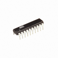
ATTINY26L-8PU Atmel, ATTINY26L-8PU Datasheet - Page 51

ATTINY26L-8PU
Manufacturer Part Number
ATTINY26L-8PU
Description
IC MCU AVR 2K 5V 8MHZ 20-DIP
Manufacturer
Atmel
Series
AVR® ATtinyr
Datasheets
1.ATTINY26-16MC.pdf
(18 pages)
2.ATTINY26-16MC.pdf
(182 pages)
3.ATTINY26L-8PU.pdf
(183 pages)
Specifications of ATTINY26L-8PU
Core Processor
AVR
Core Size
8-Bit
Speed
8MHz
Connectivity
USI
Peripherals
Brown-out Detect/Reset, POR, PWM, WDT
Number Of I /o
16
Program Memory Size
2KB (1K x 16)
Program Memory Type
FLASH
Eeprom Size
128 x 8
Ram Size
128 x 8
Voltage - Supply (vcc/vdd)
2.7 V ~ 5.5 V
Data Converters
A/D 11x10b
Oscillator Type
Internal
Operating Temperature
-40°C ~ 85°C
Package / Case
20-DIP (0.300", 7.62mm)
Processor Series
ATTINY2x
Core
AVR8
Data Bus Width
8 bit
Data Ram Size
128 B
Interface Type
2-Wire/ISP/SM-Bus/SPI/UART/USI
Maximum Clock Frequency
8 MHz
Number Of Programmable I/os
16
Number Of Timers
2
Operating Supply Voltage
2.7 V to 5.5 V
Maximum Operating Temperature
+ 85 C
Mounting Style
Through Hole
3rd Party Development Tools
EWAVR, EWAVR-BL
Development Tools By Supplier
ATAVRDRAGON, ATSTK500, ATSTK600, ATAVRISP2, ATAVRONEKIT
Minimum Operating Temperature
- 40 C
On-chip Adc
11-ch x 10-bit
Controller Family/series
AVR Tiny
No. Of I/o's
16
Eeprom Memory Size
128Byte
Ram Memory Size
128Byte
Cpu Speed
8MHz
Rohs Compliant
Yes
For Use With
ATSTK600 - DEV KIT FOR AVR/AVR32770-1007 - ISP 4PORT ATMEL AVR MCU SPI/JTAGATAVRISP2 - PROGRAMMER AVR IN SYSTEMATSTK505 - ADAPTER KIT FOR 14PIN AVR MCU
Lead Free Status / RoHS Status
Lead free / RoHS Compliant
Other names
ATTINY26L-8PJ
ATTINY26L-8PJ
ATTINY26L-8PJ
Available stocks
Company
Part Number
Manufacturer
Quantity
Price
Company:
Part Number:
ATTINY26L-8PU
Manufacturer:
Atmel
Quantity:
25 295
Part Number:
ATTINY26L-8PU
Manufacturer:
ATMEL/爱特梅尔
Quantity:
20 000
Alternate Functions Of Port B
1477F–AVR–12/04
Port B has an alternate functions for the ADC, Clocking, Timer/Counters, USI, SPI pro-
gramming and pin change interrupt. The ADC is described in “Analog to Digital
Converter” on page 94, Clocking in “AVR CPU Core” on page 6, timers in
“Timer/Counters” on page 64 and USI in “Universal Serial Interface – USI” on page 80.
Pin change interrupt triggers on pins PB7 - PB0 if interrupt is enabled and it is not
masked by the alternate functions even if the pin is configured as an output. See details
from “Pin Change Interrupt” on page 62. Pin functions in programming modes are
described in “Memory Programming” on page 107. The alternate functions are shown in
Table 26.
Table 26. Port B Pins Alternate Functions
The alternate pin configuration is as follows:
• ADC10/RESET/PCINT1 – Port B, Bit 7
ADC10: ADC Input Channel 10. Configure the port pins as inputs with the internal pull-
ups switched off to avoid the digital port function from interfering with the function of the
analog to digital converter.
RESET: External Reset input is active low and enabled by unprogramming (“1”) the
RSTDISBL Fuse. Pullup is activated and output driver and digital input are deactivated
when the pin is used as the RESET pin.
Port Pin
PB7
PB6
PB5
PB4
PB3
PB2
PB1
PB0
Alternate Functions
ADC10 (ADC Input Channel 10)
RESET (External Reset Input)
PCINT1 (Pin Change Interrupt 1)
ADC9 (ADC Input Channel 9)
INT0 (External Interrupt 0 Input)
T0 (Timer/Counter 0 External Counter Clock Input)
PCINT1 (Pin Change Interrupt 1)
ADC8 (ADC Input Channel 8)
XTAL2 (Crystal Oscillator Output)
PCINT1 (Pin Change Interrupt 1)
ADC7 (ADC Input Channel 7)
XTAL1 (Crystal Oscillator Input)
PCINT1 (Pin Change Interrupt 1)
OC1B (Timer/Counter1 PWM Output B, Timer/Counter1Output Compare B Match
Output)
PCINT0 (Pin Change Interrupt 0)
SCK (USI Clock Input/Output)
SCL (USI External Open-collector Serial Clock)
OC1B (Inverted Timer/Counter1 PWM Output B)
PCINT0 (Pin Change Interrupt 0)
DO (USI Data Output)
OC1A (Timer/Counter1 PWM Output A, Timer/Counter1 Output Compare A Match
Output)
PCINT0 (Pin Change Interrupt 0)
DI (USI Data Input)
SDA (USI Serial Data)
OC1A (Inverted Timer/Counter1 PWM Output A)
PCINT0 (Pin Change Interrupt 0)
ATtiny26(L)
51


