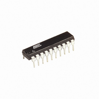
ATTINY26L-8PU Atmel, ATTINY26L-8PU Datasheet - Page 55

ATTINY26L-8PU
Manufacturer Part Number
ATTINY26L-8PU
Description
IC MCU AVR 2K 5V 8MHZ 20-DIP
Manufacturer
Atmel
Series
AVR® ATtinyr
Datasheets
1.ATTINY26-16MC.pdf
(18 pages)
2.ATTINY26-16MC.pdf
(182 pages)
3.ATTINY26L-8PU.pdf
(183 pages)
Specifications of ATTINY26L-8PU
Core Processor
AVR
Core Size
8-Bit
Speed
8MHz
Connectivity
USI
Peripherals
Brown-out Detect/Reset, POR, PWM, WDT
Number Of I /o
16
Program Memory Size
2KB (1K x 16)
Program Memory Type
FLASH
Eeprom Size
128 x 8
Ram Size
128 x 8
Voltage - Supply (vcc/vdd)
2.7 V ~ 5.5 V
Data Converters
A/D 11x10b
Oscillator Type
Internal
Operating Temperature
-40°C ~ 85°C
Package / Case
20-DIP (0.300", 7.62mm)
Processor Series
ATTINY2x
Core
AVR8
Data Bus Width
8 bit
Data Ram Size
128 B
Interface Type
2-Wire/ISP/SM-Bus/SPI/UART/USI
Maximum Clock Frequency
8 MHz
Number Of Programmable I/os
16
Number Of Timers
2
Operating Supply Voltage
2.7 V to 5.5 V
Maximum Operating Temperature
+ 85 C
Mounting Style
Through Hole
3rd Party Development Tools
EWAVR, EWAVR-BL
Development Tools By Supplier
ATAVRDRAGON, ATSTK500, ATSTK600, ATAVRISP2, ATAVRONEKIT
Minimum Operating Temperature
- 40 C
On-chip Adc
11-ch x 10-bit
Controller Family/series
AVR Tiny
No. Of I/o's
16
Eeprom Memory Size
128Byte
Ram Memory Size
128Byte
Cpu Speed
8MHz
Rohs Compliant
Yes
For Use With
ATSTK600 - DEV KIT FOR AVR/AVR32770-1007 - ISP 4PORT ATMEL AVR MCU SPI/JTAGATAVRISP2 - PROGRAMMER AVR IN SYSTEMATSTK505 - ADAPTER KIT FOR 14PIN AVR MCU
Lead Free Status / RoHS Status
Lead free / RoHS Compliant
Other names
ATTINY26L-8PJ
ATTINY26L-8PJ
ATTINY26L-8PJ
Available stocks
Company
Part Number
Manufacturer
Quantity
Price
Company:
Part Number:
ATTINY26L-8PU
Manufacturer:
Atmel
Quantity:
25 295
Part Number:
ATTINY26L-8PU
Manufacturer:
ATMEL/爱特梅尔
Quantity:
20 000
Table 28. Overriding Signals for Alternate Functions in PB3..PB0
Notes:
1477F–AVR–12/04
Signal Name
PUOE
PUOV
DDOE
DDOV
PVOE
PVOV
DIEOE
DIEOV
DI
AIO
1. Enabling of the Timer/Counter1 Compare match outputs and Timer/Counter1 PWM Outputs OC1A/OC1B and OC1A/OC1B
2. Note that the PCINT0 Interrupt is only enabled if both the Global Interrupt Flag is enabled, the PCIE0 flag in GIMSK is set
3. The Two-wire and Three-wire USI-modes are described in “Universal Serial Interface – USI” on page 80.
4. Shift clock (SCL) hold for USI is in described “Universal Serial Interface – USI” on page 80.
5. USI start up interrupt is enabled if both the Global Interrupt Flag is enabled and the USISIE flag in the USICR Register is set
6. Data Output (DO) is valid in USI Three-wire mode and the operation is described in “Universal Serial Interface – USI” on
7. Operation of the data pin SDA in USI Two-wire mode and DI in USI Three-wire mode in “Universal Serial Interface – USI” on
8. Not operator is marked with “~”.
are described in the section “8-bit Timer/Counter1” on page 67.
and the alternate function of the pin is disabled as described in “Pin Change Interrupt” on page 62.
as described in “Universal Serial Interface – USI” on page 80.
page 80.
page 80.
PB3/OC1B/PCINT0
0
0
0
0
OC1B_ENABLE
OC1B
PCINT0_ENABLE
~OC1B_ENABLE
1
PCINT0
–
(1)
(1)
(2)
•
PB2/SCK/SCL/OC1B/PCI
NT0
0
USI_TWO-WIRE
(USI_SCL_HOLD
~
USI_TWO-WIRE
DDB2 | OC1B_ENABLE
~(USI_TWO-WIRE •
DDB2) • OC1B
~(USI_TWO-WIRE |
USI_THREE-WIRE |
OC1B_ENABLE) •
PCINT0_ENABLE
USI_START_I.ENABLE
1
PCINT0, SCL, SCK
–
USI_TWO-WIRE
(8)
PORTB2) • DDB2
(3)
(3)
(3)
(4)
(2)
•
|
|
(5)
(1)
PB1/DO/OC1A/PCINT0
0
0
0
0
USI_THREE-WIRE
OC1A_ENABLE
USI_THREE-WIRE
DO
WIRE • OC1A_ENABLE
• OC1A
~(USI_THREE-WIRE |
OC1A_ENABLE) •
PCINT0_ENABLE
1
PCINT0
–
(6)
| ~USI_THREE-
(1)
(2)
(3)
(3)
|
•
(1)
PB0/DI/SDA/OC1A
0
USI_TWO-WIRE
(~SDA | ~PORTB0) •
DDB0
USI_TWO-WIRE
|
OC1A_ENABLE
~(USI_TWO-WIRE•
DDB0) •
OC1A_ENABLE
~(USI_TWO-WIRE
USI_THREE-WIRE
OC1A_ENABLE
PCINT0_ENABLE
USI_START_I.ENABLE
1
PCINT0, SDA
–
USI_TWO-WIRE
ATtiny26(L)
(1)
(1)
(1)
(3)
(3)
(3)
(2)
) •
• DDB0
• OC1A
(3)
(3)
|
|
|
(5)
55


