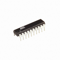
ATTINY26L-8PU Atmel, ATTINY26L-8PU Datasheet - Page 74

ATTINY26L-8PU
Manufacturer Part Number
ATTINY26L-8PU
Description
IC MCU AVR 2K 5V 8MHZ 20-DIP
Manufacturer
Atmel
Series
AVR® ATtinyr
Datasheets
1.ATTINY26-16MC.pdf
(18 pages)
2.ATTINY26-16MC.pdf
(182 pages)
3.ATTINY26L-8PU.pdf
(183 pages)
Specifications of ATTINY26L-8PU
Core Processor
AVR
Core Size
8-Bit
Speed
8MHz
Connectivity
USI
Peripherals
Brown-out Detect/Reset, POR, PWM, WDT
Number Of I /o
16
Program Memory Size
2KB (1K x 16)
Program Memory Type
FLASH
Eeprom Size
128 x 8
Ram Size
128 x 8
Voltage - Supply (vcc/vdd)
2.7 V ~ 5.5 V
Data Converters
A/D 11x10b
Oscillator Type
Internal
Operating Temperature
-40°C ~ 85°C
Package / Case
20-DIP (0.300", 7.62mm)
Processor Series
ATTINY2x
Core
AVR8
Data Bus Width
8 bit
Data Ram Size
128 B
Interface Type
2-Wire/ISP/SM-Bus/SPI/UART/USI
Maximum Clock Frequency
8 MHz
Number Of Programmable I/os
16
Number Of Timers
2
Operating Supply Voltage
2.7 V to 5.5 V
Maximum Operating Temperature
+ 85 C
Mounting Style
Through Hole
3rd Party Development Tools
EWAVR, EWAVR-BL
Development Tools By Supplier
ATAVRDRAGON, ATSTK500, ATSTK600, ATAVRISP2, ATAVRONEKIT
Minimum Operating Temperature
- 40 C
On-chip Adc
11-ch x 10-bit
Controller Family/series
AVR Tiny
No. Of I/o's
16
Eeprom Memory Size
128Byte
Ram Memory Size
128Byte
Cpu Speed
8MHz
Rohs Compliant
Yes
For Use With
ATSTK600 - DEV KIT FOR AVR/AVR32770-1007 - ISP 4PORT ATMEL AVR MCU SPI/JTAGATAVRISP2 - PROGRAMMER AVR IN SYSTEMATSTK505 - ADAPTER KIT FOR 14PIN AVR MCU
Lead Free Status / RoHS Status
Lead free / RoHS Compliant
Other names
ATTINY26L-8PJ
ATTINY26L-8PJ
ATTINY26L-8PJ
Available stocks
Company
Part Number
Manufacturer
Quantity
Price
Company:
Part Number:
ATTINY26L-8PU
Manufacturer:
Atmel
Quantity:
25 295
Part Number:
ATTINY26L-8PU
Manufacturer:
ATMEL/爱特梅尔
Quantity:
20 000
Timer/Counter1 Initialization
for Asynchronous Mode
Timer/Counter1 in PWM Mode
74
ATtiny26(L)
When the PLLE is set, the PLL is started and if needed internal RC Oscillator is started
as a PLL reference clock. If PLL is selected as a system clock source the value for this
bit is always 1.
• Bit 0 – PLOCK: PLL Lock Detector
When the PLOCK bit is set, the PLL is locked to the reference clock, and it is safe to
enable PCK for Timer/Counter1. After the PLL is enabled, it takes about 64 µs/100 µs
(typical/worst case) for the PLL to lock.
To change Timer/Counter1 to the asynchronous mode, first enable PLL, and poll the
PLOCK bit until it is set, and then set the PCKE bit.
When the PWM mode is selected, Timer/Counter1 and the Output Compare Register C
– OCR1C form a dual 8-bit, free-running and glitch-free PWM generator with outputs on
the PB1(OC1A) and PB3(OC1B) pins. Also inverted, non-overlapping outputs are avail-
able on pins PB0(OC1A) and PB2(OC1B), respectively. The non-overlapping output
pairs (OC1A - OC1A and OC1B - OC1B) are never both set at the same time. This
allows driving power switches directly. The non-overlap time is one prescaled clock
cycle, and the high time is one cycle shorter than the low time.
The non-overlap time is generated by delaying the rising edge, i.e., the positive edge is
one prescaled and one PCK cycle delayed and the negative edge is one PCK cycle
delayed in the asynchronous mode. In the synchronous mode he positive edge is one
prescaled and one CK cycle delayed and the negative edge is one CK cycle delayed.
The high time is also one prescaled cycle shorter in the both operation modes.
Figure 41. The Non-overlapping Output Pair
When the counter value match the contents of OCR1A and OCR1B, the OC1A and
O C 1 B o u t p u t s a r e s e t o r c l e a r e d a c c o r d i n g t o t h e C O M 1 A 1 / C O M 1 A 0 o r
COM1B1/COM1B0 bits in the Timer/Counter1 Control Register A – TCCR1A, as shown
in Table 35 below.
Timer/Counter1 acts as an up-counter, counting from $00 up to the value specified in
the Output Compare Register (OCR1C), and starting from $00 up again. A compare
match with OC1C will set an Overflow Interrupt Flag (TOV1) after a synchronization
delay following the compare event.
OC1x
OC1x
x = A or B
t
non-overlap
1477F–AVR–12/04


