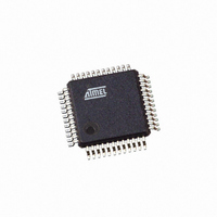
AT91SAM7S32B-AU-999 Atmel, AT91SAM7S32B-AU-999 Datasheet - Page 139

AT91SAM7S32B-AU-999
Manufacturer Part Number
AT91SAM7S32B-AU-999
Description
IC MCU ARM7 32KB FLASH 48LQFP
Manufacturer
Atmel
Series
AT91SAMr
Datasheet
1.AT91SAM7S16-MU.pdf
(779 pages)
Specifications of AT91SAM7S32B-AU-999
Core Processor
ARM7
Core Size
16/32-Bit
Speed
55MHz
Connectivity
I²C, SPI, SSC, UART/USART
Peripherals
Brown-out Detect/Reset, DMA, POR, PWM, WDT
Number Of I /o
21
Program Memory Size
32KB (32K x 8)
Program Memory Type
FLASH
Ram Size
8K x 8
Voltage - Supply (vcc/vdd)
1.65 V ~ 1.95 V
Data Converters
A/D 8x10b
Oscillator Type
Internal
Operating Temperature
-40°C ~ 85°C
Package / Case
48-LQFP
Processor Series
AT91SAMx
Core
ARM7TDMI
Data Bus Width
32 bit
Data Ram Size
8 KB
Interface Type
I2C, JTAG, SPI, USART
Maximum Clock Frequency
55 MHz
Number Of Programmable I/os
21
Operating Supply Voltage
3.3 V
Maximum Operating Temperature
+ 85 C
Mounting Style
SMD/SMT
3rd Party Development Tools
JTRACE-ARM-2M, KSK-AT91SAM7S-PL, MDK-ARM, RL-ARM, ULINK2
Development Tools By Supplier
AT91SAM-ICE, AT91-ISP, AT91SAM7S-EK
Minimum Operating Temperature
- 40 C
For Use With
AT91SAM-ICE - EMULATOR FOR AT91 ARM7/ARM9AT91SAM7S-EK - KIT EVAL FOR ARM AT91SAM7S
Lead Free Status / RoHS Status
Lead free / RoHS Compliant
Eeprom Size
-
Lead Free Status / Rohs Status
Details
Available stocks
Company
Part Number
Manufacturer
Quantity
Price
- Current page: 139 of 779
- Download datasheet (11Mb)
20.3.4.1
20.3.4.2
6175K–ATARM–30-Aug-10
Flash Read Command
Flash Write Command
This command is used to read the Flash contents. The memory map is accessible through this
command. Memory is seen as an array of words (32-bit wide). The read command can start at
any valid address in the memory plane. This address must be word-aligned. The address is
automatically incremented.
Table 20-22. Read Command
This command is used to write the Flash contents. The address transmitted must be a valid
Flash address in the memory plane.
The Flash memory plane is organized into several pages. Data to be written is stored in a load
buffer that corresponds to a Flash memory page. The load buffer is automatically flushed to the
Flash:
The Write Page command (WP) is optimized for consecutive writes. Write handshaking can be
chained; an internal address buffer is automatically increased.
Table 20-23. Write Command
Flash Write Page and Lock command (WPL) is equivalent to the Flash Write Command. How-
ever, the lock bit is automatically set at the end of the Flash write operation. As a lock region is
composed of several pages, the programmer writes to the first pages of the lock region using
Flash write commands and writes to the last page of the lock region using a Flash write and lock
command.
Flash Erase Page and Write command (EWP) is equivalent to the Flash Write Command. How-
ever, before programming the load buffer, the page is erased.
Flash Erase Page and Write the Lock command (EWPL) combines EWP and WPL
commands.
Read/Write
Write
Write
Read
Read
...
Read
Read/Write
Write
Write
Write
Write
Write
Write
• before access to any page than the current one
• at the end of the number of words transmitted
DR Data
(Number of Words to Read) << 16 | READ
Address
Memory [address]
Memory [address+4]
...
Memory [address+(Number of Words to Read - 1)* 4]
DR Data
(Number of Words to Write) << 16 | (WP or WPL or EWP or EWPL)
Address
Memory [address]
Memory [address+4]
Memory [address+8]
Memory [address+(Number of Words to Write - 1)* 4]
AT91SAM7S Series Preliminary
139
Related parts for AT91SAM7S32B-AU-999
Image
Part Number
Description
Manufacturer
Datasheet
Request
R

Part Number:
Description:
Manufacturer:
ATMEL Corporation
Datasheet:

Part Number:
Description:
IC ARM7 MCU 32BIT 32K 48LQFP
Manufacturer:
Atmel
Datasheet:

Part Number:
Description:
AT91 ARM Thumb-based Microcontrollers
Manufacturer:
ATMEL [ATMEL Corporation]
Datasheet:

Part Number:
Description:
IC ARM7 MCU FLASH 32K 48QFN
Manufacturer:
Atmel
Datasheet:

Part Number:
Description:
IC MCU ARM7 32KB FLASH 48LQFP
Manufacturer:
Atmel
Datasheet:

Part Number:
Description:
IC MCU ARM7 32KB FLASH 48-VQFN
Manufacturer:
Atmel
Datasheet:

Part Number:
Description:
DEV KIT FOR AVR/AVR32
Manufacturer:
Atmel
Datasheet:

Part Number:
Description:
INTERVAL AND WIPE/WASH WIPER CONTROL IC WITH DELAY
Manufacturer:
ATMEL Corporation
Datasheet:

Part Number:
Description:
Low-Voltage Voice-Switched IC for Hands-Free Operation
Manufacturer:
ATMEL Corporation
Datasheet:

Part Number:
Description:
MONOLITHIC INTEGRATED FEATUREPHONE CIRCUIT
Manufacturer:
ATMEL Corporation
Datasheet:

Part Number:
Description:
AM-FM Receiver IC U4255BM-M
Manufacturer:
ATMEL Corporation
Datasheet:

Part Number:
Description:
Monolithic Integrated Feature Phone Circuit
Manufacturer:
ATMEL Corporation
Datasheet:

Part Number:
Description:
Multistandard Video-IF and Quasi Parallel Sound Processing
Manufacturer:
ATMEL Corporation
Datasheet:


