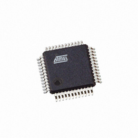
AT91SAM7S32B-AU-999 Atmel, AT91SAM7S32B-AU-999 Datasheet - Page 740

AT91SAM7S32B-AU-999
Manufacturer Part Number
AT91SAM7S32B-AU-999
Description
IC MCU ARM7 32KB FLASH 48LQFP
Manufacturer
Atmel
Series
AT91SAMr
Datasheet
1.AT91SAM7S16-MU.pdf
(779 pages)
Specifications of AT91SAM7S32B-AU-999
Core Processor
ARM7
Core Size
16/32-Bit
Speed
55MHz
Connectivity
I²C, SPI, SSC, UART/USART
Peripherals
Brown-out Detect/Reset, DMA, POR, PWM, WDT
Number Of I /o
21
Program Memory Size
32KB (32K x 8)
Program Memory Type
FLASH
Ram Size
8K x 8
Voltage - Supply (vcc/vdd)
1.65 V ~ 1.95 V
Data Converters
A/D 8x10b
Oscillator Type
Internal
Operating Temperature
-40°C ~ 85°C
Package / Case
48-LQFP
Processor Series
AT91SAMx
Core
ARM7TDMI
Data Bus Width
32 bit
Data Ram Size
8 KB
Interface Type
I2C, JTAG, SPI, USART
Maximum Clock Frequency
55 MHz
Number Of Programmable I/os
21
Operating Supply Voltage
3.3 V
Maximum Operating Temperature
+ 85 C
Mounting Style
SMD/SMT
3rd Party Development Tools
JTRACE-ARM-2M, KSK-AT91SAM7S-PL, MDK-ARM, RL-ARM, ULINK2
Development Tools By Supplier
AT91SAM-ICE, AT91-ISP, AT91SAM7S-EK
Minimum Operating Temperature
- 40 C
For Use With
AT91SAM-ICE - EMULATOR FOR AT91 ARM7/ARM9AT91SAM7S-EK - KIT EVAL FOR ARM AT91SAM7S
Lead Free Status / RoHS Status
Lead free / RoHS Compliant
Eeprom Size
-
Lead Free Status / Rohs Status
Details
Available stocks
Company
Part Number
Manufacturer
Quantity
Price
- Current page: 740 of 779
- Download datasheet (11Mb)
40.21.3.4
40.21.3.5
40.21.4
40.21.4.1
40.21.5
40.21.5.1
40.21.5.2
40.21.5.3
740
AT91SAM7S Series Preliminary
Real Time Timer (RTT)
Serial Peripheral Interface (SPI)
PWM: Constraints on Duty Cycle Value
PWM: Behavior of CHIDx Status Bits in the PWM_SR Register
RTT: Possible Event Loss when Reading RTT_SR
SPI: Software Reset Must be Written Twice
20. SPI: Pulse Generation on SPCK
SPI: Bad tx_ready behavior when CSAAT=1 and SCBR = 1
Setting Channel Duty Cycle Register (PWM_CDTYx) at 0 in center aligned mode or at 0 or 1 in
left aligned mode may change the polarity of the signal.
Do not set PWM_CDTYx at 0 in center aligned mode.
Do not set PWM_CDTYx at 0 or 1 in left aligned mode.
Erratic behavior of the CHIDx status bit in the PWM_SR Register. When a channel is disabled
by writing in the PWM_DIS Register just after enabling it (before completion of a Clock Period of
the clock selected for the channel), the PWM line is internally disabled but the CHIDx status bit
in the PWM_SR stays at 1.
Do not disable a channel before completion of one period of the selected clock.
If an event (RTTINC or ALMS) occurs within the same slow clock cycle during which the
RTT_SR is read, the corresponding bit might be cleared. This can lead to the loss of this event.
The software must handle the RTT event as an interrupt and should not poll RTT_SR.
If a software reset (SWRSTin the SPI Control Register) is performed, the SPI may not work
properly (the clock is enabled before the chip select.
The SPI Control Register field, SWRST needs to be written twice to be set correctly.
In Master Mode, there is an additional pulse generated on SPCK when the SPI is configured as
follows:
None.
If the SPI is programmed with CSAAT = 1, SCBR(baudrate) = 1 and two transfers are performed
consecutively on the same slave with an IDLE state between them, the tx_ready signal does not
rise after the second data has been transferred in the shifter. This can imply for example, that
the second data is sent twice.
Problem Fix/Workaround
Problem Fix/Workaround
Problem Fix/Workaround:
Problem Fix/Workaround
Problem Fix/Workaround
– The Baudrate is odd and different from 1
– The Polarity is set to 1
– The Phase is set to 0
6175K–ATARM–30-Aug-10
Related parts for AT91SAM7S32B-AU-999
Image
Part Number
Description
Manufacturer
Datasheet
Request
R

Part Number:
Description:
Manufacturer:
ATMEL Corporation
Datasheet:

Part Number:
Description:
IC ARM7 MCU 32BIT 32K 48LQFP
Manufacturer:
Atmel
Datasheet:

Part Number:
Description:
AT91 ARM Thumb-based Microcontrollers
Manufacturer:
ATMEL [ATMEL Corporation]
Datasheet:

Part Number:
Description:
IC ARM7 MCU FLASH 32K 48QFN
Manufacturer:
Atmel
Datasheet:

Part Number:
Description:
IC MCU ARM7 32KB FLASH 48LQFP
Manufacturer:
Atmel
Datasheet:

Part Number:
Description:
IC MCU ARM7 32KB FLASH 48-VQFN
Manufacturer:
Atmel
Datasheet:

Part Number:
Description:
DEV KIT FOR AVR/AVR32
Manufacturer:
Atmel
Datasheet:

Part Number:
Description:
INTERVAL AND WIPE/WASH WIPER CONTROL IC WITH DELAY
Manufacturer:
ATMEL Corporation
Datasheet:

Part Number:
Description:
Low-Voltage Voice-Switched IC for Hands-Free Operation
Manufacturer:
ATMEL Corporation
Datasheet:

Part Number:
Description:
MONOLITHIC INTEGRATED FEATUREPHONE CIRCUIT
Manufacturer:
ATMEL Corporation
Datasheet:

Part Number:
Description:
AM-FM Receiver IC U4255BM-M
Manufacturer:
ATMEL Corporation
Datasheet:

Part Number:
Description:
Monolithic Integrated Feature Phone Circuit
Manufacturer:
ATMEL Corporation
Datasheet:

Part Number:
Description:
Multistandard Video-IF and Quasi Parallel Sound Processing
Manufacturer:
ATMEL Corporation
Datasheet:


