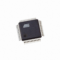
AT91SAM7S32B-AU-999 Atmel, AT91SAM7S32B-AU-999 Datasheet - Page 725

AT91SAM7S32B-AU-999
Manufacturer Part Number
AT91SAM7S32B-AU-999
Description
IC MCU ARM7 32KB FLASH 48LQFP
Manufacturer
Atmel
Series
AT91SAMr
Datasheet
1.AT91SAM7S16-MU.pdf
(779 pages)
Specifications of AT91SAM7S32B-AU-999
Core Processor
ARM7
Core Size
16/32-Bit
Speed
55MHz
Connectivity
I²C, SPI, SSC, UART/USART
Peripherals
Brown-out Detect/Reset, DMA, POR, PWM, WDT
Number Of I /o
21
Program Memory Size
32KB (32K x 8)
Program Memory Type
FLASH
Ram Size
8K x 8
Voltage - Supply (vcc/vdd)
1.65 V ~ 1.95 V
Data Converters
A/D 8x10b
Oscillator Type
Internal
Operating Temperature
-40°C ~ 85°C
Package / Case
48-LQFP
Processor Series
AT91SAMx
Core
ARM7TDMI
Data Bus Width
32 bit
Data Ram Size
8 KB
Interface Type
I2C, JTAG, SPI, USART
Maximum Clock Frequency
55 MHz
Number Of Programmable I/os
21
Operating Supply Voltage
3.3 V
Maximum Operating Temperature
+ 85 C
Mounting Style
SMD/SMT
3rd Party Development Tools
JTRACE-ARM-2M, KSK-AT91SAM7S-PL, MDK-ARM, RL-ARM, ULINK2
Development Tools By Supplier
AT91SAM-ICE, AT91-ISP, AT91SAM7S-EK
Minimum Operating Temperature
- 40 C
For Use With
AT91SAM-ICE - EMULATOR FOR AT91 ARM7/ARM9AT91SAM7S-EK - KIT EVAL FOR ARM AT91SAM7S
Lead Free Status / RoHS Status
Lead free / RoHS Compliant
Eeprom Size
-
Lead Free Status / Rohs Status
Details
Available stocks
Company
Part Number
Manufacturer
Quantity
Price
- Current page: 725 of 779
- Download datasheet (11Mb)
40.19.8.3
40.19.9
40.19.9.1
40.19.9.2
40.19.9.3
6175K–ATARM–30-Aug-10
Two-wire Interface (TWI)
SSC: Transmitter Limitations in Slave Mode
TWI: Clock Divider
TWI: Software Reset
TWI: Disabling Does not Operate Correctly
If TK is programmed as an input and TF is programmed as an output and requested to be set to
low/high during data emission, the Frame Synchro signal is generated one bit clock period after
the data start and one data bit is lost. This problem does not exist when generating a periodic
synchro.
The data need to be delayed for one bit clock period with an external assembly.
In the following schematic, TD, TK and NRST are AT91SAM7S signals, TXD is the delayed data
to connect to the device.
The value of CLDIV x 2
be less than or equal to 8191⋅
None.
When a software reset is performed during a frame and when TWCK is low, it is impossible to
initiate a new transfer in READ or WRITE mode.
None.
Any transfer in progress is immediately frozen if the Control Register (TWI_CR) is written with
the bit MSDIS at 1. Furthermore, the status bits TXCOMP and TXRDY in the Status Register
(TWI_SR) are not reset.
Problem Fix/Workaround
Problem Fix/Workaround
Problem Fix/Workaround
CKDIV
must be less than or equal to 8191, the value of CHDIV x 2
AT91SAM7S Series Preliminary
CKDIV
must
725
Related parts for AT91SAM7S32B-AU-999
Image
Part Number
Description
Manufacturer
Datasheet
Request
R

Part Number:
Description:
Manufacturer:
ATMEL Corporation
Datasheet:

Part Number:
Description:
IC ARM7 MCU 32BIT 32K 48LQFP
Manufacturer:
Atmel
Datasheet:

Part Number:
Description:
AT91 ARM Thumb-based Microcontrollers
Manufacturer:
ATMEL [ATMEL Corporation]
Datasheet:

Part Number:
Description:
IC ARM7 MCU FLASH 32K 48QFN
Manufacturer:
Atmel
Datasheet:

Part Number:
Description:
IC MCU ARM7 32KB FLASH 48LQFP
Manufacturer:
Atmel
Datasheet:

Part Number:
Description:
IC MCU ARM7 32KB FLASH 48-VQFN
Manufacturer:
Atmel
Datasheet:

Part Number:
Description:
DEV KIT FOR AVR/AVR32
Manufacturer:
Atmel
Datasheet:

Part Number:
Description:
INTERVAL AND WIPE/WASH WIPER CONTROL IC WITH DELAY
Manufacturer:
ATMEL Corporation
Datasheet:

Part Number:
Description:
Low-Voltage Voice-Switched IC for Hands-Free Operation
Manufacturer:
ATMEL Corporation
Datasheet:

Part Number:
Description:
MONOLITHIC INTEGRATED FEATUREPHONE CIRCUIT
Manufacturer:
ATMEL Corporation
Datasheet:

Part Number:
Description:
AM-FM Receiver IC U4255BM-M
Manufacturer:
ATMEL Corporation
Datasheet:

Part Number:
Description:
Monolithic Integrated Feature Phone Circuit
Manufacturer:
ATMEL Corporation
Datasheet:

Part Number:
Description:
Multistandard Video-IF and Quasi Parallel Sound Processing
Manufacturer:
ATMEL Corporation
Datasheet:


