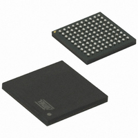
ATMEGA640-16CU Atmel, ATMEGA640-16CU Datasheet - Page 158

ATMEGA640-16CU
Manufacturer Part Number
ATMEGA640-16CU
Description
IC MCU AVR 64K FLASH 100-CBGA
Manufacturer
Atmel
Series
AVR® ATmegar
Specifications of ATMEGA640-16CU
Core Processor
AVR
Core Size
8-Bit
Speed
16MHz
Connectivity
EBI/EMI, I²C, SPI, UART/USART
Peripherals
Brown-out Detect/Reset, POR, PWM, WDT
Number Of I /o
86
Program Memory Size
64KB (32K x 16)
Program Memory Type
FLASH
Eeprom Size
4K x 8
Ram Size
8K x 8
Voltage - Supply (vcc/vdd)
2.7 V ~ 5.5 V
Data Converters
A/D 16x10b
Oscillator Type
Internal
Operating Temperature
-40°C ~ 85°C
Package / Case
100-TFBGA
Processor Series
ATMEGA64x
Core
AVR8
Data Bus Width
8 bit
Data Ram Size
8 KB
Interface Type
2-Wire, SPI, USART
Maximum Clock Frequency
16 MHz
Number Of Programmable I/os
86
Number Of Timers
6
Maximum Operating Temperature
+ 85 C
Mounting Style
SMD/SMT
3rd Party Development Tools
EWAVR, EWAVR-BL
Development Tools By Supplier
ATAVRDRAGON, ATSTK500, ATSTK600, ATAVRISP2, ATAVRONEKIT
Minimum Operating Temperature
- 40 C
On-chip Adc
10 bit, 16 Channel
For Use With
ATSTK600-TQFP100 - STK600 SOCKET/ADAPTER 100-TQFP770-1007 - ISP 4PORT ATMEL AVR MCU SPI/JTAGATAVRISP2 - PROGRAMMER AVR IN SYSTEMATSTK503 - STARTER KIT AVR EXP MODULE 100P
Lead Free Status / RoHS Status
Lead free / RoHS Compliant
Available stocks
Company
Part Number
Manufacturer
Quantity
Price
- Current page: 158 of 444
- Download datasheet (10Mb)
16.11 Register Description
16.11.1
16.11.2
16.11.3
16.11.4
2549M–AVR–09/10
TCCR1A – Timer/Counter 1 Control Register A
TCCR3A – Timer/Counter 3 Control Register A
TCCR4A – Timer/Counter 4 Control Register A
TCCR5A – Timer/Counter 5 Control Register A
•
•
•
The COMnA1:0, COMnB1:0, and COMnC1:0 control the output compare pins (OCnA, OCnB,
and OCnC respectively) behavior. If one or both of the COMnA1:0 bits are written to one, the
OCnA output overrides the normal port functionality of the I/O pin it is connected to. If one or
both of the COMnB1:0 bits are written to one, the OCnB output overrides the normal port func-
tionality of the I/O pin it is connected to. If one or both of the COMnC1:0 bits are written to one,
the OCnC output overrides the normal port functionality of the I/O pin it is connected to. How-
ever, note that the Data Direction Register (DDR) bit corresponding to the OCnA, OCnB or
OCnC pin must be set in order to enable the output driver.
When the OCnA, OCnB or OCnC is connected to the pin, the function of the COMnx1:0 bits is
dependent of the WGMn3:0 bits setting.
tionality when the WGMn3:0 bits are set to a normal or a CTC mode (non-PWM).
Bit
(0x80)
Read/Write
Initial Value
Bit
(0x90)
Read/Write
Initial Value
Bit
(0xA0)
Read/Write
Initial Value
Bit
(0x120)
Read/Write
Initial Value
Bit 7:6 – COMnA1:0: Compare Output Mode for Channel A
Bit 5:4 – COMnB1:0: Compare Output Mode for Channel B
Bit 3:2 – COMnC1:0: Compare Output Mode for Channel C
COM1A1
COM3A1
COM4A1
COM5A1
R/W
R/W
R/W
R/W
7
0
7
0
7
0
7
0
COM1A0
COM3A0
COM4A0
COM5A0
R/W
R/W
R/W
R/W
6
0
6
0
6
0
6
0
ATmega640/1280/1281/2560/2561
COM1B1
COM3B1
COM4B1
COM5B1
R/W
R/W
R/W
R/W
5
0
5
0
5
0
5
0
Table 16-3 on page 159
COM1B0
COM3B0
COM4B0
COM5B0
R/W
R/W
R/W
R/W
4
0
4
0
4
0
4
0
COM1C1
COM3C1
COM4C1
COM5C1
R/W
R/W
R/W
R/W
3
0
3
0
3
0
3
0
COM1C0
COM3C0
COM4C0
COM5C0
R/W
R/W
R/W
R/W
2
0
2
0
2
0
2
0
shows the COMnx1:0 bit func-
WGM11
WGM31
WGM41
WGM51
R/W
R/W
R/W
R/W
1
0
1
0
1
0
1
0
WGM10
WGM30
WGM40
WGM50
R/W
R/W
R/W
R/W
0
0
0
0
0
0
0
0
TCCR1A
TCCR3A
TCCR4A
TCCR5A
158
Related parts for ATMEGA640-16CU
Image
Part Number
Description
Manufacturer
Datasheet
Request
R

Part Number:
Description:
Manufacturer:
Atmel Corporation
Datasheet:

Part Number:
Description:
IC MCU AVR 64K FLASH 100-TQFP
Manufacturer:
Atmel
Datasheet:

Part Number:
Description:
MCU AVR 64K FLASH 16MHZ 100TQFP
Manufacturer:
Atmel
Datasheet:

Part Number:
Description:
MCU AVR 64K FLASH 16MHZ 100CBGA
Manufacturer:
Atmel
Datasheet:

Part Number:
Description:
Manufacturer:
Atmel Corporation
Datasheet:

Part Number:
Description:
Manufacturer:
ATMEL Corporation
Datasheet:

Part Number:
Description:
Manufacturer:
ATMEL Corporation
Datasheet:

Part Number:
Description:
IC AVR MCU 64K 16MHZ 5V 64TQFP
Manufacturer:
Atmel
Datasheet:

Part Number:
Description:
IC AVR MCU 64K 16MHZ 5V 64-QFN
Manufacturer:
Atmel
Datasheet:

Part Number:
Description:
IC AVR MCU 64K 16MHZ COM 64-TQFP
Manufacturer:
Atmel
Datasheet:

Part Number:
Description:
IC AVR MCU 64K 16MHZ IND 64-TQFP
Manufacturer:
Atmel
Datasheet:

Part Number:
Description:
IC AVR MCU 64K 16MHZ COM 64-QFN
Manufacturer:
Atmel
Datasheet:

Part Number:
Description:
MCU AVR 64KB FLASH 16MHZ 64TQFP
Manufacturer:
Atmel
Datasheet:

Part Number:
Description:
MCU AVR 64KB FLASH 16MHZ 64QFN
Manufacturer:
Atmel
Datasheet:


