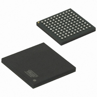
ATMEGA640-16CU Atmel, ATMEGA640-16CU Datasheet - Page 172

ATMEGA640-16CU
Manufacturer Part Number
ATMEGA640-16CU
Description
IC MCU AVR 64K FLASH 100-CBGA
Manufacturer
Atmel
Series
AVR® ATmegar
Specifications of ATMEGA640-16CU
Core Processor
AVR
Core Size
8-Bit
Speed
16MHz
Connectivity
EBI/EMI, I²C, SPI, UART/USART
Peripherals
Brown-out Detect/Reset, POR, PWM, WDT
Number Of I /o
86
Program Memory Size
64KB (32K x 16)
Program Memory Type
FLASH
Eeprom Size
4K x 8
Ram Size
8K x 8
Voltage - Supply (vcc/vdd)
2.7 V ~ 5.5 V
Data Converters
A/D 16x10b
Oscillator Type
Internal
Operating Temperature
-40°C ~ 85°C
Package / Case
100-TFBGA
Processor Series
ATMEGA64x
Core
AVR8
Data Bus Width
8 bit
Data Ram Size
8 KB
Interface Type
2-Wire, SPI, USART
Maximum Clock Frequency
16 MHz
Number Of Programmable I/os
86
Number Of Timers
6
Maximum Operating Temperature
+ 85 C
Mounting Style
SMD/SMT
3rd Party Development Tools
EWAVR, EWAVR-BL
Development Tools By Supplier
ATAVRDRAGON, ATSTK500, ATSTK600, ATAVRISP2, ATAVRONEKIT
Minimum Operating Temperature
- 40 C
On-chip Adc
10 bit, 16 Channel
For Use With
ATSTK600-TQFP100 - STK600 SOCKET/ADAPTER 100-TQFP770-1007 - ISP 4PORT ATMEL AVR MCU SPI/JTAGATAVRISP2 - PROGRAMMER AVR IN SYSTEMATSTK503 - STARTER KIT AVR EXP MODULE 100P
Lead Free Status / RoHS Status
Lead free / RoHS Compliant
Available stocks
Company
Part Number
Manufacturer
Quantity
Price
- Current page: 172 of 444
- Download datasheet (10Mb)
18. Output Compare Modulator (OCM1C0A)
18.1
18.2
2549M–AVR–09/10
Overview
Description
The Output Compare Modulator (OCM) allows generation of waveforms modulated with a carrier
frequency. The modulator uses the outputs from the Output Compare Unit C of the 16-bit
Timer/Counter1 and the Output Compare Unit of the 8-bit Timer/Counter0. For more details
about these Timer/Counters see
bit Timer/Counter2 with PWM and Asynchronous Operation” on page
Figure 18-1. Output Compare Modulator, Block Diagram
When the modulator is enabled, the two output compare channels are modulated together as
shown in the block diagram (see
The Output Compare unit 1C and Output Compare unit 2 shares the PB7 port pin for output. The
outputs of the Output Compare units (OC1C and OC0A) overrides the normal PORTB7 Register
when one of them is enabled (that is, when COMnx1:0 is not equal to zero). When both OC1C
and OC0A are enabled at the same time, the modulator is automatically enabled.
The functional equivalent schematic of the modulator is shown on
includes part of the Timer/Counter units and the port B pin 7 output driver circuit.
Figure 18-2. Output Compare Modulator, Schematic
( From Waveform Generator )
( From Waveform Generator )
COMA01
COMA00
COM1C1
COM1C0
Timer/Counter 1
Timer/Counter 0
PORTB7
D
OC1C
D
OC0A
D
Q
Q
Q
ATmega640/1280/1281/2560/2561
“Timer/Counter 0, 1, 3, 4, and 5 Prescaler” on page 169
Figure
DATABUS
18-1).
OC1C
OC0A
Modulator
0
1
DDRB7
D
Figure
Q
1
0
174.
OC0A / PB7
OC1C /
18-2. The schematic
Pin
Vcc
OC0A/ PB7
and
OC1C /
Pin
172
“8-
Related parts for ATMEGA640-16CU
Image
Part Number
Description
Manufacturer
Datasheet
Request
R

Part Number:
Description:
Manufacturer:
Atmel Corporation
Datasheet:

Part Number:
Description:
IC MCU AVR 64K FLASH 100-TQFP
Manufacturer:
Atmel
Datasheet:

Part Number:
Description:
MCU AVR 64K FLASH 16MHZ 100TQFP
Manufacturer:
Atmel
Datasheet:

Part Number:
Description:
MCU AVR 64K FLASH 16MHZ 100CBGA
Manufacturer:
Atmel
Datasheet:

Part Number:
Description:
Manufacturer:
Atmel Corporation
Datasheet:

Part Number:
Description:
Manufacturer:
ATMEL Corporation
Datasheet:

Part Number:
Description:
Manufacturer:
ATMEL Corporation
Datasheet:

Part Number:
Description:
IC AVR MCU 64K 16MHZ 5V 64TQFP
Manufacturer:
Atmel
Datasheet:

Part Number:
Description:
IC AVR MCU 64K 16MHZ 5V 64-QFN
Manufacturer:
Atmel
Datasheet:

Part Number:
Description:
IC AVR MCU 64K 16MHZ COM 64-TQFP
Manufacturer:
Atmel
Datasheet:

Part Number:
Description:
IC AVR MCU 64K 16MHZ IND 64-TQFP
Manufacturer:
Atmel
Datasheet:

Part Number:
Description:
IC AVR MCU 64K 16MHZ COM 64-QFN
Manufacturer:
Atmel
Datasheet:

Part Number:
Description:
MCU AVR 64KB FLASH 16MHZ 64TQFP
Manufacturer:
Atmel
Datasheet:

Part Number:
Description:
MCU AVR 64KB FLASH 16MHZ 64QFN
Manufacturer:
Atmel
Datasheet:


