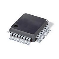
ST7FLITE49K2T6TR STMicroelectronics, ST7FLITE49K2T6TR Datasheet - Page 103

ST7FLITE49K2T6TR
Manufacturer Part Number
ST7FLITE49K2T6TR
Description
IC MCU 8BIT 8K FLASH 32LQFP
Manufacturer
STMicroelectronics
Series
ST7r
Datasheet
1.ST7FLITE49K2T6TR.pdf
(245 pages)
Specifications of ST7FLITE49K2T6TR
Core Processor
ST7
Core Size
8-Bit
Speed
8MHz
Connectivity
I²C, SPI
Peripherals
LVD, POR, PWM, WDT
Number Of I /o
24
Program Memory Size
8KB (8K x 8)
Program Memory Type
FLASH
Eeprom Size
256 x 8
Ram Size
384 x 8
Voltage - Supply (vcc/vdd)
2.4 V ~ 5.5 V
Data Converters
A/D 10x10b
Oscillator Type
Internal
Operating Temperature
-40°C ~ 85°C
Package / Case
32-LQFP
Processor Series
ST7FLITE4x
Core
ST7
Data Bus Width
8 bit
Data Ram Size
384 B
Interface Type
I2C, SPI
Maximum Clock Frequency
8 MHz
Number Of Programmable I/os
24
Number Of Timers
4
Maximum Operating Temperature
+ 85 C
Mounting Style
SMD/SMT
Development Tools By Supplier
ST7FLITE-SK/RAIS, ST7FLI49M-D/RAIS, STX-RLINK
Minimum Operating Temperature
- 40 C
On-chip Adc
10 bit, 10 Channel
For Use With
497-8399 - BOARD EVAL ST7LITE49M/STLED316S497-5858 - EVAL BOARD PLAYBACK ST7FLITE
Lead Free Status / RoHS Status
Lead free / RoHS Compliant
Available stocks
Company
Part Number
Manufacturer
Quantity
Price
Company:
Part Number:
ST7FLITE49K2T6TR
Manufacturer:
STMicroelectronics
Quantity:
10 000
- Current page: 103 of 245
- Download datasheet (4Mb)
ST7LITE49K2
Bit 4 = BP2EN Break 2 pin enable bit
Bits 3:2 = Reserved, must be kept cleared
Bit 1 = SWBR2 Switch Break for counter 2 bit
Bit 0 = SWBR1 Switch Break for counter 1 bit
PWMx duty cycle register High (DCRxH)
Reset value: 0000 0000 (00h)
Bits 15:12 = Reserved.
PWMx duty cycle register Low (DCRxL)
Reset value: 0000 0000 (00h)
Bits 11:0 = DCRx[11:0] PWMx Duty Cycle Value: this 12-bit value is written by software. It
defines the duty cycle of the corresponding PWM output signal (see
In PWM mode (OEx=1 in the PWMCR register) the DCR[11:0] bits define the duty cycle of
the PWMx output signal (see
be compared with the 12-bit upcounter value.
DCR7
15
This bit is read/write by software and cleared by hardware after Reset.
0: BREAK2 pin disabled
1: BREAK2 pin enabled
This bit is read/write by software. While BREN2 is set, it selects BA1 or BA2 to control
PWM2/3 if ENCNTR2 bit is set.
0: BA1 selected
1: BA2 selected
This bit is read/write by software. While BREN1 is set, it selects BA1 or BA2 to control
PWM0/1 by default and also PWM2/3 if ENCNTR2 bit is reset.
0: BA1 selected
1: BA2 selected
0
7
DCR6
0
DCR5
0
Figure
40). In Output Compare mode, they define the value to
DCR4
0
Read/write
Read/write
DCR11
DCR3
DCR10
DCR2
Figure
On-chip peripherals
DCR1
DCR9
40).
DCR0
DCR8
103/245
0
8
Related parts for ST7FLITE49K2T6TR
Image
Part Number
Description
Manufacturer
Datasheet
Request
R

Part Number:
Description:
STMicroelectronics [RIPPLE-CARRY BINARY COUNTER/DIVIDERS]
Manufacturer:
STMicroelectronics
Datasheet:

Part Number:
Description:
STMicroelectronics [LIQUID-CRYSTAL DISPLAY DRIVERS]
Manufacturer:
STMicroelectronics
Datasheet:

Part Number:
Description:
BOARD EVAL FOR MEMS SENSORS
Manufacturer:
STMicroelectronics
Datasheet:

Part Number:
Description:
NPN TRANSISTOR POWER MODULE
Manufacturer:
STMicroelectronics
Datasheet:

Part Number:
Description:
TURBOSWITCH ULTRA-FAST HIGH VOLTAGE DIODE
Manufacturer:
STMicroelectronics
Datasheet:

Part Number:
Description:
Manufacturer:
STMicroelectronics
Datasheet:

Part Number:
Description:
DIODE / SCR MODULE
Manufacturer:
STMicroelectronics
Datasheet:

Part Number:
Description:
DIODE / SCR MODULE
Manufacturer:
STMicroelectronics
Datasheet:

Part Number:
Description:
Search -----> STE16N100
Manufacturer:
STMicroelectronics
Datasheet:

Part Number:
Description:
Search ---> STE53NA50
Manufacturer:
STMicroelectronics
Datasheet:

Part Number:
Description:
NPN Transistor Power Module
Manufacturer:
STMicroelectronics
Datasheet:

Part Number:
Description:
DIODE / SCR MODULE
Manufacturer:
STMicroelectronics
Datasheet:


