ST7FLITE49K2T6TR STMicroelectronics, ST7FLITE49K2T6TR Datasheet - Page 148
ST7FLITE49K2T6TR
Manufacturer Part Number
ST7FLITE49K2T6TR
Description
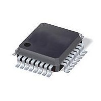
IC MCU 8BIT 8K FLASH 32LQFP
Manufacturer
STMicroelectronics
Series
ST7r
Datasheet
1.ST7FLITE49K2T6TR.pdf
(245 pages)
Specifications of ST7FLITE49K2T6TR
Core Processor
ST7
Core Size
8-Bit
Speed
8MHz
Connectivity
I²C, SPI
Peripherals
LVD, POR, PWM, WDT
Number Of I /o
24
Program Memory Size
8KB (8K x 8)
Program Memory Type
FLASH
Eeprom Size
256 x 8
Ram Size
384 x 8
Voltage - Supply (vcc/vdd)
2.4 V ~ 5.5 V
Data Converters
A/D 10x10b
Oscillator Type
Internal
Operating Temperature
-40°C ~ 85°C
Package / Case
32-LQFP
Processor Series
ST7FLITE4x
Core
ST7
Data Bus Width
8 bit
Data Ram Size
384 B
Interface Type
I2C, SPI
Maximum Clock Frequency
8 MHz
Number Of Programmable I/os
24
Number Of Timers
4
Maximum Operating Temperature
+ 85 C
Mounting Style
SMD/SMT
Development Tools By Supplier
ST7FLITE-SK/RAIS, ST7FLI49M-D/RAIS, STX-RLINK
Minimum Operating Temperature
- 40 C
On-chip Adc
10 bit, 10 Channel
For Use With
497-8399 - BOARD EVAL ST7LITE49M/STLED316S497-5858 - EVAL BOARD PLAYBACK ST7FLITE
Lead Free Status / RoHS Status
Lead free / RoHS Compliant
Available stocks
Company
Part Number
Manufacturer
Quantity
Price
Company:

Part Number:
ST7FLITE49K2T6TR
Manufacturer:
STMicroelectronics
Quantity:
10 000


On-chip peripherals
11.5.7
Note:
Note:
148/245
Register description
I
Reset value: 0000 0000 (00h)
Bits 7:6 = Reserved. Forced to 0 by hardware.
Bit 5 = PE Peripheral Enable bit
When PE=0, all the bits of the CR register and the SR register except the Stop bit are reset.
All outputs are released while PE=0
When PE=1, the corresponding I/O pins are selected by hardware as alternate functions.
To enable the I
activates the interface (only PE is set).
Bit 4 = ENGC Enable General Call bit
In accordance with the I
only receive data. It will not transmit data to the master.
Bit 3 = START Generation of a Start condition bit. This bit is set and cleared by software. It
is also cleared by hardware when the interface is disabled (PE=0) or when the Start
condition is sent (with interrupt generation if ITE=1).
●
●
Bit 2 = ACK Acknowledge enable bit
2
C control register (I2CCR)
This bit is set and cleared by software.
0: Peripheral disabled
1: Master/Slave capability
This bit is set and cleared by software. It is also cleared by hardware when the interface
is disabled (PE=0). The 00h General Call address is acknowledged (01h ignored).
0: General Call disabled
1: General Call enabled
In master mode:
0: No start generation
1: Repeated start generation
In slave mode:
0: No start generation
1: Start generation when the bus is free
This bit is set and cleared by software. It is also cleared by hardware when the interface
is disabled (PE=0).
0: No acknowledge returned
1: Acknowledge returned after an address byte or a data byte is received
7
0
2
C interface, write the CR register TWICE with PE=1 as the first write only
0
2
C standard, when GCAL addressing is enabled, an I
PE
ENGC
Read / Write
START
ACK
STOP
ST7LITE49K2
2
C slave can
ITE
0
Related parts for ST7FLITE49K2T6TR
Image
Part Number
Description
Manufacturer
Datasheet
Request
R

Part Number:
Description:
STMicroelectronics [RIPPLE-CARRY BINARY COUNTER/DIVIDERS]
Manufacturer:
STMicroelectronics
Datasheet:
Part Number:
Description:
STMicroelectronics [LIQUID-CRYSTAL DISPLAY DRIVERS]
Manufacturer:
STMicroelectronics
Datasheet:

Part Number:
Description:
BOARD EVAL FOR MEMS SENSORS
Manufacturer:
STMicroelectronics
Datasheet:
Part Number:
Description:
NPN TRANSISTOR POWER MODULE
Manufacturer:
STMicroelectronics
Datasheet:
Part Number:
Description:
TURBOSWITCH ULTRA-FAST HIGH VOLTAGE DIODE
Manufacturer:
STMicroelectronics
Datasheet:
Part Number:
Description:
Manufacturer:
STMicroelectronics
Datasheet:
Part Number:
Description:
DIODE / SCR MODULE
Manufacturer:
STMicroelectronics
Datasheet:
Part Number:
Description:
DIODE / SCR MODULE
Manufacturer:
STMicroelectronics
Datasheet:
Part Number:
Description:
Search -----> STE16N100
Manufacturer:
STMicroelectronics
Datasheet:
Part Number:
Description:
Search ---> STE53NA50
Manufacturer:
STMicroelectronics
Datasheet:
Part Number:
Description:
NPN Transistor Power Module
Manufacturer:
STMicroelectronics
Datasheet:
Part Number:
Description:
DIODE / SCR MODULE
Manufacturer:
STMicroelectronics
Datasheet: