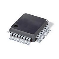
ST7FLITE49K2T6TR STMicroelectronics, ST7FLITE49K2T6TR Datasheet - Page 127

ST7FLITE49K2T6TR
Manufacturer Part Number
ST7FLITE49K2T6TR
Description
IC MCU 8BIT 8K FLASH 32LQFP
Manufacturer
STMicroelectronics
Series
ST7r
Datasheet
1.ST7FLITE49K2T6TR.pdf
(245 pages)
Specifications of ST7FLITE49K2T6TR
Core Processor
ST7
Core Size
8-Bit
Speed
8MHz
Connectivity
I²C, SPI
Peripherals
LVD, POR, PWM, WDT
Number Of I /o
24
Program Memory Size
8KB (8K x 8)
Program Memory Type
FLASH
Eeprom Size
256 x 8
Ram Size
384 x 8
Voltage - Supply (vcc/vdd)
2.4 V ~ 5.5 V
Data Converters
A/D 10x10b
Oscillator Type
Internal
Operating Temperature
-40°C ~ 85°C
Package / Case
32-LQFP
Processor Series
ST7FLITE4x
Core
ST7
Data Bus Width
8 bit
Data Ram Size
384 B
Interface Type
I2C, SPI
Maximum Clock Frequency
8 MHz
Number Of Programmable I/os
24
Number Of Timers
4
Maximum Operating Temperature
+ 85 C
Mounting Style
SMD/SMT
Development Tools By Supplier
ST7FLITE-SK/RAIS, ST7FLI49M-D/RAIS, STX-RLINK
Minimum Operating Temperature
- 40 C
On-chip Adc
10 bit, 10 Channel
For Use With
497-8399 - BOARD EVAL ST7LITE49M/STLED316S497-5858 - EVAL BOARD PLAYBACK ST7FLITE
Lead Free Status / RoHS Status
Lead free / RoHS Compliant
Available stocks
Company
Part Number
Manufacturer
Quantity
Price
Company:
Part Number:
ST7FLITE49K2T6TR
Manufacturer:
STMicroelectronics
Quantity:
10 000
- Current page: 127 of 245
- Download datasheet (4Mb)
ST7LITE49K2
Note:
1
2
3
4
5
The OCF1 bit cannot be set by hardware in one pulse mode but the OCF2 bit can generate
an output compare interrupt.
When the pulse width modulation (PWM) and one pulse mode (OPM) bits are both set, the
PWM mode is the only active one.
If OLVL1 = OLVL2 a continuous signal is seen on the OCMP1 pin.
The ICAP1 pin can not be used to perform input capture. The ICAP2 pin can be used to
perform input capture (ICF2 can be set and IC2R can be loaded) but the user must take
care that the counter is reset each time a valid edge occurs on the ICAP1 pin and ICF1 can
also generates interrupt if ICIE is set.
When one pulse mode is used OC1R is dedicated to this mode. Nevertheless OC2R and
OCF2 can be used to indicate a period of time has been elapsed but cannot generate an
output waveform because the level OLVL2 is dedicated to the one pulse mode.
Figure 66. One pulse mode timing example
1. IEDG1 = 1, OC1R = 2ED0h, OLVL1 = 0, OLVL2 = 1
Figure 67. Pulse width modulation mode timing example
1. OC1R = 2ED0h, OC2R = 34E2, OLVL1 = 0, OLVL2 = 1
Pulse width modulation mode
Pulse width modulation (PWM) mode enables the generation of a signal with a frequency
and pulse length determined by the value of the OC1R and OC2R registers.
Pulse width modulation mode uses the complete output compare 1 function plus the OC2R
register, and so this functionality can not be used when PWM mode is activated.
In PWM mode, double buffering is implemented on the output compare registers. Any new
values written in the OC1R and OC2R registers are loaded in their respective shadow
registers (double buffer) only at the end of the PWM period (OC2) to avoid spikes on the
PWM output pin (OCMP1). The shadow registers contain the reference values for
comparison in PWM ‘double buffering’ mode.
Counter 34E2
OCMP1
Counter
OCMP1
ICAP1
IC1R
01F8
Compare2
FFFC FFFD FFFE
FFFC FFFD FFFE
OLVL2
OLVL2
01F8
2ED0 2ED1 2ED2
2ED0 2ED1 2ED2
Compare1
Compare1
OLVL1
OLVL1
2ED3
FFFC FFFD
2ED3
Compare2
On-chip peripherals
34E2 FFFC
OLVL2
OLVL2
127/245
Related parts for ST7FLITE49K2T6TR
Image
Part Number
Description
Manufacturer
Datasheet
Request
R

Part Number:
Description:
STMicroelectronics [RIPPLE-CARRY BINARY COUNTER/DIVIDERS]
Manufacturer:
STMicroelectronics
Datasheet:

Part Number:
Description:
STMicroelectronics [LIQUID-CRYSTAL DISPLAY DRIVERS]
Manufacturer:
STMicroelectronics
Datasheet:

Part Number:
Description:
BOARD EVAL FOR MEMS SENSORS
Manufacturer:
STMicroelectronics
Datasheet:

Part Number:
Description:
NPN TRANSISTOR POWER MODULE
Manufacturer:
STMicroelectronics
Datasheet:

Part Number:
Description:
TURBOSWITCH ULTRA-FAST HIGH VOLTAGE DIODE
Manufacturer:
STMicroelectronics
Datasheet:

Part Number:
Description:
Manufacturer:
STMicroelectronics
Datasheet:

Part Number:
Description:
DIODE / SCR MODULE
Manufacturer:
STMicroelectronics
Datasheet:

Part Number:
Description:
DIODE / SCR MODULE
Manufacturer:
STMicroelectronics
Datasheet:

Part Number:
Description:
Search -----> STE16N100
Manufacturer:
STMicroelectronics
Datasheet:

Part Number:
Description:
Search ---> STE53NA50
Manufacturer:
STMicroelectronics
Datasheet:

Part Number:
Description:
NPN Transistor Power Module
Manufacturer:
STMicroelectronics
Datasheet:

Part Number:
Description:
DIODE / SCR MODULE
Manufacturer:
STMicroelectronics
Datasheet:


