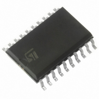
ST62T60CM6 STMicroelectronics, ST62T60CM6 Datasheet - Page 38

ST62T60CM6
Manufacturer Part Number
ST62T60CM6
Description
IC MCU 8BIT OTP/EPROM 20 PSOIC
Manufacturer
STMicroelectronics
Series
ST6r
Datasheet
1.ST62T60CB6.pdf
(83 pages)
Specifications of ST62T60CM6
Core Processor
ST6
Core Size
8-Bit
Speed
8MHz
Connectivity
SPI
Peripherals
LED, LVD, POR, WDT
Number Of I /o
13
Program Memory Size
3.8KB (3.8K x 8)
Program Memory Type
OTP
Eeprom Size
128 x 8
Ram Size
128 x 8
Voltage - Supply (vcc/vdd)
3 V ~ 6 V
Data Converters
A/D 7x8b
Oscillator Type
Internal
Operating Temperature
-40°C ~ 85°C
Package / Case
20-SOIC (7.5mm Width)
Processor Series
ST62T6x
Core
ST6
Data Bus Width
8 bit
Data Ram Size
128 B
Interface Type
SPI
Maximum Clock Frequency
8 MHz
Number Of Programmable I/os
13
Number Of Timers
2
Operating Supply Voltage
3 V to 6 V
Maximum Operating Temperature
+ 85 C
Mounting Style
SMD/SMT
Development Tools By Supplier
ST622XC-KIT/110, ST62GP-EMU2, ST62E2XC-EPB/110, ST62E6XC-EPB/US, STREALIZER-II
Minimum Operating Temperature
- 40 C
On-chip Adc
8 bit
Lead Free Status / RoHS Status
Lead free / RoHS Compliant
Other names
497-2102-5
Available stocks
Company
Part Number
Manufacturer
Quantity
Price
Company:
Part Number:
ST62T60CM6
Manufacturer:
LT
Quantity:
492
I/O PORTS (Cont’d)
4.1.2 Safe I/O State Switching Sequence
Switching the I/O ports from one state to another
should be done in a sequence which ensures that
no unwanted side effects can occur. The recom-
mended safe transitions are illustrated in
24. All other transitions are potentially risky and
should be avoided when changing the I/O operat-
ing mode, as it is most likely that undesirable side-
effects will be experienced, such as spurious inter-
rupt generation or two pins shorted together by the
analog multiplexer.
Single bit instructions (SET, RES, INC and DEC)
should be used with great caution on Ports Data
registers, since these instructions make an implicit
read and write back of the entire register. In port
input mode, however, the data register reads from
the input pins directly, and not from the data regis-
ter latches. Since data register information in input
mode is used to set the characteristics of the input
pin (interrupt, pull-up, analog input), these may be
unintentionally reprogrammed depending on the
state of the input pins. As a general rule, it is better
to limit the use of single bit instructions on data
registers to when the whole (8-bit) port is in output
mode. In the case of inputs or of mixed inputs and
Figure 24. Diagram showing Safe I/O State Transitions
Note *. xxx = DDR, OR, DR Bits respectively
Interrupt
pull-up
Input
pull-up (Reset
state)
Output
Open Drain
Output
Push-pull
010*
000
100
110
Figure
ST6253C ST6263C ST6263B ST6260C ST6260B
outputs, it is advisable to keep a copy of the data
register in RAM. Single bit instructions may then
be used on the RAM copy, after which the whole
copy register can be written to the port data regis-
ter:
SET bit, datacopy
LD a, datacopy
LD DRA, a
Warning: Care must also be taken to not use in-
structions that act on a whole port register (INC,
DEC, or read operations) when all 8 bits are not
available on the device. Unavailable bits must be
masked by software (AND instruction).
The WAIT and STOP instructions allow the
ST62xx to be used in situations where low power
consumption is needed. The lowest power con-
sumption is achieved by configuring I/Os in input
mode with well-defined logic levels.
The user must take care not to switch outputs with
heavy loads during the conversion of one of the
analog inputs in order to avoid any disturbance to
the conversion.
011
001
101
111
Open Drain
Push-pull
Analog
Output
Output
Input
Input
38/83


