HD64F2612FA20 Renesas Electronics America, HD64F2612FA20 Datasheet - Page 18
HD64F2612FA20
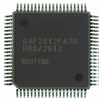
Manufacturer Part Number
HD64F2612FA20
Description
IC H8S MCU FLASH 128K 80QFP
Manufacturer
Renesas Electronics America
Series
H8® H8S/2600r
Specifications of HD64F2612FA20
Core Processor
H8S/2600
Core Size
16-Bit
Speed
20MHz
Connectivity
CAN, SCI
Peripherals
POR, PWM, WDT
Number Of I /o
43
Program Memory Size
128KB (128K x 8)
Program Memory Type
FLASH
Ram Size
4K x 8
Voltage - Supply (vcc/vdd)
4.5 V ~ 5.5 V
Data Converters
A/D 12x10b
Oscillator Type
Internal
Operating Temperature
-20°C ~ 75°C
Package / Case
80-QFP
Lead Free Status / RoHS Status
Contains lead / RoHS non-compliant
Eeprom Size
-
Available stocks
Company
Part Number
Manufacturer
Quantity
Price

Part Number:
HD64F2612FA20
Manufacturer:
RENESAS/瑞萨
Quantity:
20 000
Part Number:
HD64F2612FA20J
Manufacturer:
RENESAS/瑞萨
Quantity:
20 000


12.5 Usage Notes ....................................................................................................................... 301
Section 13 Watchdog Timer ..............................................................................303
13.1 Features .............................................................................................................................. 303
13.2 Register Descriptions ......................................................................................................... 304
13.3 Operation............................................................................................................................ 308
13.4 Interrupts ............................................................................................................................ 309
13.5 Usage Notes ....................................................................................................................... 309
Section 14 Serial Communication Interface (SCI) ............................................313
14.1 Features .............................................................................................................................. 313
14.2 Input/Output Pins ............................................................................................................... 315
14.3 Register Descriptions ......................................................................................................... 315
Rev. 7.00 Sep. 11, 2009 Page xvi of xxxiv
REJ09B0211-0700
12.4.3 Sample Setup Procedure for Normal Pulse Output............................................... 293
12.4.4 Example of Normal Pulse Output (Example of Five-Phase Pulse Output)........... 294
12.4.5 Non-Overlapping Pulse Output............................................................................. 295
12.4.6 Sample Setup Procedure for Non-Overlapping Pulse Output ............................... 297
12.4.7 Example of Non-Overlapping Pulse Output
12.4.8 Inverted Pulse Output ........................................................................................... 300
12.4.9 Pulse Output Triggered by Input Capture ............................................................. 301
12.5.1 Module Stop Mode Setting ................................................................................... 301
12.5.2 Operation of Pulse Output Pins............................................................................. 301
13.2.1 Timer Counter (TCNT)......................................................................................... 304
13.2.2 Timer Control/Status Register (TCSR) ................................................................. 305
13.2.3 Reset Control/Status Register (RSTCSR) ............................................................. 307
13.3.1 Watchdog Timer Mode ......................................................................................... 308
13.3.2 Interval Timer Mode ............................................................................................. 308
13.5.1 Notes on Register Access...................................................................................... 309
13.5.2 Contention between Timer Counter (TCNT) Write and Increment ...................... 310
13.5.3 Changing Value of CKS2 to CKS0....................................................................... 311
13.5.4 Switching between Watchdog Timer Mode and Interval Timer Mode................. 311
13.5.5 Internal Reset in Watchdog Timer Mode.............................................................. 311
13.5.6 OVF Flag Clearing in Intervel Timer Mode ......................................................... 311
14.3.1 Receive Shift Register (RSR) ............................................................................... 316
14.3.2 Receive Data Register (RDR) ............................................................................... 316
14.3.3 Transmit Data Register (TDR).............................................................................. 316
14.3.4 Transmit Shift Register (TSR) .............................................................................. 316
14.3.5 Serial Mode Register (SMR)................................................................................. 317
14.3.6 Serial Control Register (SCR)............................................................................... 321
14.3.7 Serial Status Register (SSR) ................................................................................. 324
(Example of Four-Phase Complementary Non-Overlapping Output)................... 298
Related parts for HD64F2612FA20
Image
Part Number
Description
Manufacturer
Datasheet
Request
R


Part Number:
Description:
KIT STARTER FOR M16C/29
Manufacturer:
Renesas Electronics America
Datasheet:

Part Number:
Description:
KIT STARTER FOR R8C/2D
Manufacturer:
Renesas Electronics America
Datasheet:

Part Number:
Description:
R0K33062P STARTER KIT
Manufacturer:
Renesas Electronics America
Datasheet:

Part Number:
Description:
KIT STARTER FOR R8C/23 E8A
Manufacturer:
Renesas Electronics America
Datasheet:

Part Number:
Description:
KIT STARTER FOR R8C/25
Manufacturer:
Renesas Electronics America
Datasheet:

Part Number:
Description:
KIT STARTER H8S2456 SHARPE DSPLY
Manufacturer:
Renesas Electronics America
Datasheet:

Part Number:
Description:
KIT STARTER FOR R8C38C
Manufacturer:
Renesas Electronics America
Datasheet:

Part Number:
Description:
KIT STARTER FOR R8C35C
Manufacturer:
Renesas Electronics America
Datasheet:

Part Number:
Description:
KIT STARTER FOR R8CL3AC+LCD APPS
Manufacturer:
Renesas Electronics America
Datasheet:
Part Number:
Description:
KIT STARTER FOR RX610
Manufacturer:
Renesas Electronics America
Datasheet:

Part Number:
Description:
KIT STARTER FOR R32C/118
Manufacturer:
Renesas Electronics America
Datasheet:

Part Number:
Description:
KIT DEV RSK-R8C/26-29
Manufacturer:
Renesas Electronics America
Datasheet:

Part Number:
Description:
KIT STARTER FOR SH7124
Manufacturer:
Renesas Electronics America
Datasheet:

Part Number:
Description:
KIT STARTER FOR H8SX/1622
Manufacturer:
Renesas Electronics America
Datasheet: