HD64F2612FA20 Renesas Electronics America, HD64F2612FA20 Datasheet - Page 28
HD64F2612FA20
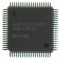
Manufacturer Part Number
HD64F2612FA20
Description
IC H8S MCU FLASH 128K 80QFP
Manufacturer
Renesas Electronics America
Series
H8® H8S/2600r
Specifications of HD64F2612FA20
Core Processor
H8S/2600
Core Size
16-Bit
Speed
20MHz
Connectivity
CAN, SCI
Peripherals
POR, PWM, WDT
Number Of I /o
43
Program Memory Size
128KB (128K x 8)
Program Memory Type
FLASH
Ram Size
4K x 8
Voltage - Supply (vcc/vdd)
4.5 V ~ 5.5 V
Data Converters
A/D 12x10b
Oscillator Type
Internal
Operating Temperature
-20°C ~ 75°C
Package / Case
80-QFP
Lead Free Status / RoHS Status
Contains lead / RoHS non-compliant
Eeprom Size
-
Available stocks
Company
Part Number
Manufacturer
Quantity
Price

Part Number:
HD64F2612FA20
Manufacturer:
RENESAS/瑞萨
Quantity:
20 000
Part Number:
HD64F2612FA20J
Manufacturer:
RENESAS/瑞萨
Quantity:
20 000


Figure 14.2
Figure 14.3
Figure 14.4
Figure 14.5
Figure 14.6
Figure 14.7
Figure 14.8
Figure 14.9
Figure 14.9
Figure 14.10 Example of Communication Using Multiprocessor Format
Figure 14.11 Sample Multiprocessor Serial Transmission Flowchart ......................................... 351
Figure 14.12 Example of SCI Operation in Reception
Figure 14.13 Sample Multiprocessor Serial Reception Flowchart (1)......................................... 353
Figure 14.13 Sample Multiprocessor Serial Reception Flowchart (2)......................................... 354
Figure 14.14 Data Format in Synchronous Communication (For LSB-First) ............................. 355
Figure 14.15 Sample SCI Initialization Flowchart ...................................................................... 356
Figure 14.16 Sample SCI Transmission Operation in Clocked Synchronous Mode ................... 358
Figure 14.17 Sample Serial Transmission Flowchart .................................................................. 359
Figure 14.18 Example of SCI Operation in Reception ................................................................ 360
Figure 14.19 Sample Serial Reception Flowchart ....................................................................... 361
Figure 14.20 Sample Flowchart of Simultaneous Serial Transmit and Receive Operations ....... 363
Figure 14.21 Schematic Diagram of Smart Card Interface Pin Connections............................... 364
Figure 14.22 Normal Smart Card Interface Data Format ............................................................ 365
Figure 14.23 Direct Convention (SDIR = SINV = O/E = 0) ....................................................... 365
Figure 14.24 Inverse Convention (SDIR = SINV = O/E = 1) ..................................................... 366
Figure 14.25 Receive Data Sampling Timing in Smart Card Mode
Figure 14.26 Retransfer Operation in SCI Transmit Mode ......................................................... 370
Figure 14.27 TEND Flag Generation Timing in Transmission Operation .................................. 370
Figure 14.28 Example of Transmission Processing Flow ........................................................... 371
Figure 14.29 Retransfer Operation in SCI Receive Mode........................................................... 372
Figure 14.30 Example of Reception Processing Flow................................................................. 373
Figure 14.31 Timing for Fixing Clock Output Level .................................................................. 373
Figure 14.32 Clock Halt and Restart Procedure .......................................................................... 374
Figure 14.33 Sample Transmission using DTC in Clocked Synchronous Mode......................... 378
Rev. 7.00 Sep. 11, 2009 Page xxvi of xxxiv
REJ09B0211-0700
Data Format in Asynchronous Communication
(Example with 8-Bit Data, Parity, Two Stop Bits)................................................. 338
Receive Data Sampling Timing in Asynchronous Mode ....................................... 340
Relationship between Output Clock and Transfer Data Phase
(Asynchronous Mode)............................................................................................ 341
Sample SCI Initialization Flowchart ...................................................................... 342
Example of Operation in Transmission in Asynchronous Mode
(Example with 8-Bit Data, Parity, One Stop Bit) ................................................... 343
Sample Serial Transmission Flowchart .................................................................. 344
Example of SCI Operation in Reception
(Example with 8-Bit Data, Parity, One Stop Bit) ................................................... 345
Sample Serial Reception Data Flowchart (1) ......................................................... 347
Sample Serial Reception Data Flowchart (2) ......................................................... 348
(Transmission of Data H'AA to Receiving Station A) ........................................... 350
(Example with 8-Bit Data, Multiprocessor Bit, One Stop Bit)............................... 352
(Using Clock of 372 Times the Transfer Rate) ...................................................... 368
Related parts for HD64F2612FA20
Image
Part Number
Description
Manufacturer
Datasheet
Request
R


Part Number:
Description:
KIT STARTER FOR M16C/29
Manufacturer:
Renesas Electronics America
Datasheet:

Part Number:
Description:
KIT STARTER FOR R8C/2D
Manufacturer:
Renesas Electronics America
Datasheet:

Part Number:
Description:
R0K33062P STARTER KIT
Manufacturer:
Renesas Electronics America
Datasheet:

Part Number:
Description:
KIT STARTER FOR R8C/23 E8A
Manufacturer:
Renesas Electronics America
Datasheet:

Part Number:
Description:
KIT STARTER FOR R8C/25
Manufacturer:
Renesas Electronics America
Datasheet:

Part Number:
Description:
KIT STARTER H8S2456 SHARPE DSPLY
Manufacturer:
Renesas Electronics America
Datasheet:

Part Number:
Description:
KIT STARTER FOR R8C38C
Manufacturer:
Renesas Electronics America
Datasheet:

Part Number:
Description:
KIT STARTER FOR R8C35C
Manufacturer:
Renesas Electronics America
Datasheet:

Part Number:
Description:
KIT STARTER FOR R8CL3AC+LCD APPS
Manufacturer:
Renesas Electronics America
Datasheet:
Part Number:
Description:
KIT STARTER FOR RX610
Manufacturer:
Renesas Electronics America
Datasheet:

Part Number:
Description:
KIT STARTER FOR R32C/118
Manufacturer:
Renesas Electronics America
Datasheet:

Part Number:
Description:
KIT DEV RSK-R8C/26-29
Manufacturer:
Renesas Electronics America
Datasheet:

Part Number:
Description:
KIT STARTER FOR SH7124
Manufacturer:
Renesas Electronics America
Datasheet:

Part Number:
Description:
KIT STARTER FOR H8SX/1622
Manufacturer:
Renesas Electronics America
Datasheet: