HD64F2612FA20 Renesas Electronics America, HD64F2612FA20 Datasheet - Page 508
HD64F2612FA20
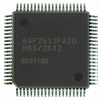
Manufacturer Part Number
HD64F2612FA20
Description
IC H8S MCU FLASH 128K 80QFP
Manufacturer
Renesas Electronics America
Series
H8® H8S/2600r
Specifications of HD64F2612FA20
Core Processor
H8S/2600
Core Size
16-Bit
Speed
20MHz
Connectivity
CAN, SCI
Peripherals
POR, PWM, WDT
Number Of I /o
43
Program Memory Size
128KB (128K x 8)
Program Memory Type
FLASH
Ram Size
4K x 8
Voltage - Supply (vcc/vdd)
4.5 V ~ 5.5 V
Data Converters
A/D 12x10b
Oscillator Type
Internal
Operating Temperature
-20°C ~ 75°C
Package / Case
80-QFP
Lead Free Status / RoHS Status
Contains lead / RoHS non-compliant
Eeprom Size
-
Available stocks
Company
Part Number
Manufacturer
Quantity
Price

Part Number:
HD64F2612FA20
Manufacturer:
RENESAS/瑞萨
Quantity:
20 000
Part Number:
HD64F2612FA20J
Manufacturer:
RENESAS/瑞萨
Quantity:
20 000


Section 18 ROM
18.8.2
When erasing flash memory, the erase/erase-verify flowchart shown in figure 18.10 should be
followed.
1. Prewriting (setting erase block data to all 0s) is not necessary.
2. Erasing is performed in block units. Make only a single-bit specification in the erase block
3. The time during which the E bit is set to 1 is the flash memory erase time.
4. The watchdog timer (WDT) is set to prevent overerasing due to program runaway, etc. An
5. For a dummy write to a verify address, write 1-byte data H'FF to an address whose lower two
6. If the read data is not erased successfully, set erase mode again, and repeat the erase/erase-
18.8.3
All interrupts, including the NMI interrupt, are disabled while flash memory is being programmed
or erased, or while the boot program is executing, for the following three reasons:
1. Interrupt during programming/erasing may cause a violation of the programming or erasing
2. If interrupt exception handling starts before the vector address is written or during
3. If an interrupt occurs during boot program execution, normal boot mode sequence cannot be
Rev. 7.00 Sep. 11, 2009 Page 472 of 566
REJ09B0211-0700
registers (EBR1 and EBR2). To erase multiple blocks, each block must be erased in turn.
overflow cycle of approximately 19.8 ms is allowed.
bits are B'00. Verify data can be read in longwords from the address to which a dummy write
was performed.
verify sequence as before. The maximum number of repetitions of the erase/erase-verify
sequence is 100.
algorithm, with the result that normal operation cannot be assured.
programming/erasing, a correct vector cannot be fetched and the CPU malfunctions.
carried out.
Erase/Erase-Verify
Interrupt Handling when Programming/Erasing Flash Memory
Related parts for HD64F2612FA20
Image
Part Number
Description
Manufacturer
Datasheet
Request
R


Part Number:
Description:
KIT STARTER FOR M16C/29
Manufacturer:
Renesas Electronics America
Datasheet:

Part Number:
Description:
KIT STARTER FOR R8C/2D
Manufacturer:
Renesas Electronics America
Datasheet:

Part Number:
Description:
R0K33062P STARTER KIT
Manufacturer:
Renesas Electronics America
Datasheet:

Part Number:
Description:
KIT STARTER FOR R8C/23 E8A
Manufacturer:
Renesas Electronics America
Datasheet:

Part Number:
Description:
KIT STARTER FOR R8C/25
Manufacturer:
Renesas Electronics America
Datasheet:

Part Number:
Description:
KIT STARTER H8S2456 SHARPE DSPLY
Manufacturer:
Renesas Electronics America
Datasheet:

Part Number:
Description:
KIT STARTER FOR R8C38C
Manufacturer:
Renesas Electronics America
Datasheet:

Part Number:
Description:
KIT STARTER FOR R8C35C
Manufacturer:
Renesas Electronics America
Datasheet:

Part Number:
Description:
KIT STARTER FOR R8CL3AC+LCD APPS
Manufacturer:
Renesas Electronics America
Datasheet:
Part Number:
Description:
KIT STARTER FOR RX610
Manufacturer:
Renesas Electronics America
Datasheet:

Part Number:
Description:
KIT STARTER FOR R32C/118
Manufacturer:
Renesas Electronics America
Datasheet:

Part Number:
Description:
KIT DEV RSK-R8C/26-29
Manufacturer:
Renesas Electronics America
Datasheet:

Part Number:
Description:
KIT STARTER FOR SH7124
Manufacturer:
Renesas Electronics America
Datasheet:

Part Number:
Description:
KIT STARTER FOR H8SX/1622
Manufacturer:
Renesas Electronics America
Datasheet: