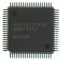
HD64F2612FA20 Renesas Electronics America, HD64F2612FA20 Datasheet - Page 27

HD64F2612FA20
Manufacturer Part Number
HD64F2612FA20
Description
IC H8S MCU FLASH 128K 80QFP
Manufacturer
Renesas Electronics America
Series
H8® H8S/2600r
Specifications of HD64F2612FA20
Core Processor
H8S/2600
Core Size
16-Bit
Speed
20MHz
Connectivity
CAN, SCI
Peripherals
POR, PWM, WDT
Number Of I /o
43
Program Memory Size
128KB (128K x 8)
Program Memory Type
FLASH
Ram Size
4K x 8
Voltage - Supply (vcc/vdd)
4.5 V ~ 5.5 V
Data Converters
A/D 12x10b
Oscillator Type
Internal
Operating Temperature
-20°C ~ 75°C
Package / Case
80-QFP
Lead Free Status / RoHS Status
Contains lead / RoHS non-compliant
Eeprom Size
-
Available stocks
Company
Part Number
Manufacturer
Quantity
Price
Part Number:
HD64F2612FA20
Manufacturer:
RENESAS/瑞萨
Quantity:
20 000
Part Number:
HD64F2612FA20J
Manufacturer:
RENESAS/瑞萨
Quantity:
20 000
- Current page: 27 of 606
- Download datasheet (4Mb)
Figure 11.3
Figure 11.4
Figure 11.5
Figure 11.6
Figure 11.7
Figure 11.8
Figure 11.9
Figure 11.10 TCNT Counter Clearing Timing ............................................................................ 264
Figure 11.11 TDCNT Operation Timing..................................................................................... 265
Figure 11.12 Dead Time Generation Timing............................................................................... 266
Figure 11.13 Buffer Operation Timing........................................................................................ 267
Figure 11.14 TGI Interrupt Timing ............................................................................................. 268
Figure 11.15 Timing of Status Flag Clearing by CPU................................................................. 269
Figure 11.16 Timing of Status Flag Clearing by DTC Controller ............................................... 269
Figure 11.17 Contention between Buffer Register Write and Compare Match........................... 270
Figure 11.18 Contention between Compare Register Write and Compare Match....................... 271
Figure 11.19 Error Case in Writing Operation ............................................................................ 272
Figure 11.20 Output Waveform Caused by Dead Time Limitation............................................. 273
Figure 11.21 Block Diagram of POE .......................................................................................... 274
Figure 11.22 Low Level Detection Operation ............................................................................. 279
Section 12 Programmable Pulse Generator (PPG)
Figure 12.1
Figure 12.2
Figure 12.3
Figure 12.4
Figure 12.5
Figure 12.6
Figure 12.7
Figure 12.8
Figure 12.9
Figure 12.10 Inverted Pulse Output (Example) ........................................................................... 300
Figure 12.11 Pulse Output Triggered by Input Capture (Example)............................................. 301
Section 13 Watchdog Timer
Figure 13.1
Figure 13.2
Figure 13.3
Section 14 Serial Communication Interface (SCI)
Figure 14.1
MMT Canceling Procedure.................................................................................... 255
Example of TCNT Count Operation ...................................................................... 256
Examples of Counter and Register Operations....................................................... 257
Example of PWM Waveform Generation .............................................................. 260
Example of TCNT Counter Clearing ..................................................................... 261
Example of Toggle Output Waveform Synchronized with PWM Period .............. 262
Count Timing ......................................................................................................... 264
Block Diagram of PPG........................................................................................... 282
PPG Output Operation ........................................................................................... 291
Timing of Transfer and Output of NDR Contents (Example) ................................ 292
Setup Procedure for Normal Pulse Output (Example) ........................................... 293
Normal Pulse Output Example (Five-Phase Pulse Output) .................................... 294
Non-Overlapping Pulse Output .............................................................................. 295
Non-Overlapping Operation and NDR Write Timing ............................................ 296
Setup Procedure for Non-Overlapping Pulse Output (Example)............................ 297
Non-Overlapping Pulse Output Example (Four-Phase Complementary)............... 298
Block Diagram of WDT......................................................................................... 304
Writing to TCNT, TCSR, and RSTCSR (Example for WDT0) ............................. 310
Contention between TCNT Write and Increment................................................... 310
Block Diagram of SCI............................................................................................ 314
Rev. 7.00 Sep. 11, 2009 Page xxv of xxxiv
REJ09B0211-0700
Related parts for HD64F2612FA20
Image
Part Number
Description
Manufacturer
Datasheet
Request
R

Part Number:
Description:
KIT STARTER FOR M16C/29
Manufacturer:
Renesas Electronics America
Datasheet:

Part Number:
Description:
KIT STARTER FOR R8C/2D
Manufacturer:
Renesas Electronics America
Datasheet:

Part Number:
Description:
R0K33062P STARTER KIT
Manufacturer:
Renesas Electronics America
Datasheet:

Part Number:
Description:
KIT STARTER FOR R8C/23 E8A
Manufacturer:
Renesas Electronics America
Datasheet:

Part Number:
Description:
KIT STARTER FOR R8C/25
Manufacturer:
Renesas Electronics America
Datasheet:

Part Number:
Description:
KIT STARTER H8S2456 SHARPE DSPLY
Manufacturer:
Renesas Electronics America
Datasheet:

Part Number:
Description:
KIT STARTER FOR R8C38C
Manufacturer:
Renesas Electronics America
Datasheet:

Part Number:
Description:
KIT STARTER FOR R8C35C
Manufacturer:
Renesas Electronics America
Datasheet:

Part Number:
Description:
KIT STARTER FOR R8CL3AC+LCD APPS
Manufacturer:
Renesas Electronics America
Datasheet:

Part Number:
Description:
KIT STARTER FOR RX610
Manufacturer:
Renesas Electronics America
Datasheet:

Part Number:
Description:
KIT STARTER FOR R32C/118
Manufacturer:
Renesas Electronics America
Datasheet:

Part Number:
Description:
KIT DEV RSK-R8C/26-29
Manufacturer:
Renesas Electronics America
Datasheet:

Part Number:
Description:
KIT STARTER FOR SH7124
Manufacturer:
Renesas Electronics America
Datasheet:

Part Number:
Description:
KIT STARTER FOR H8SX/1622
Manufacturer:
Renesas Electronics America
Datasheet:


