HD6417034AFI20 Renesas Electronics America, HD6417034AFI20 Datasheet - Page 192
HD6417034AFI20
Manufacturer Part Number
HD6417034AFI20
Description
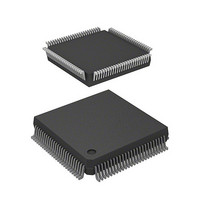
IC SUPERH MPU ROMLESS 112QFP
Manufacturer
Renesas Electronics America
Series
SuperH® SH7030r
Datasheet
1.HD6417034AFI20.pdf
(689 pages)
Specifications of HD6417034AFI20
Core Processor
SH-1
Core Size
32-Bit
Speed
20MHz
Connectivity
EBI/EMI, SCI
Peripherals
DMA, POR, PWM, WDT
Number Of I /o
32
Program Memory Type
ROMless
Ram Size
4K x 8
Voltage - Supply (vcc/vdd)
4.5 V ~ 5.5 V
Data Converters
A/D 8x10b
Oscillator Type
Internal
Operating Temperature
-20°C ~ 75°C
Package / Case
112-QFP
Lead Free Status / RoHS Status
Contains lead / RoHS non-compliant
Eeprom Size
-
Program Memory Size
-
Available stocks
Company
Part Number
Manufacturer
Quantity
Price
Company:

Part Number:
HD6417034AFI20
Manufacturer:
Renesas Electronics America
Quantity:
10 000
Company:
Part Number:
HD6417034AFI20V
Manufacturer:
Renesas Electronics America
Quantity:
10 000


Section 8 Bus State Controller (BSC)
8.6.3
The byte access control signals when the address/data multiplexed I/O space is being accessed are
of two types (WRH, WRL, A0, or WR, HBS, LBS), just as for byte access control of external
memory space access. These types can be selected using the BAS bit in BCR. See section 8.4.3,
Byte Access Control, for details.
8.7
The BSC can check and generate parity for data input and output to or from the DRAM space of
area 1 and the external memory space of area 2.
To check and generate parity, select the space (DRAM space only, or DRAM space and area 2) for
which parity is to be checked and generated using the parity check enable bits (PCHK1 and
PCHK0) in the parity control register, and select odd or even parity with the parity polarity bit
(PEO).
When data is input from the space selected with the PCHK1 and PCHK0 bits, the BSC checks the
PEO bit to see if the polarity of the DPH pin input (upper byte parity data) is accurate for the
AD15–AD8 pin input (upper byte data) or if the DPL pin input (lower byte parity data) is accurate
for the AD7–AD0 pin input (lower byte data). If the check indicates that either the upper or lower
byte parity is incorrect, a parity error interrupt is produced (PEI).
When outputting data to the space selected with the PCHK1 and PCHK0 bits, the BSC outputs
parity data output of the polarity set in the PEO bit from the DPH pin for the AD15–AD8 pin
output (upper byte data) or from the DPL pin for the AD7–AD0 pin input (lower byte data) using
the same timing as the data output.
The BSC is also able to force parity output for use in testing the system's parity error check
function. When the parity force output bit (PFRC) in PCR is set to 1, a high level is forcibly output
from the DPH and DPL pins when data is output to the space selected with the PCHK1 and
PCHK0 bits.
Rev. 7.00 Jan 31, 2006 page 164 of 658
REJ09B0272-0700
Byte Access Control
Parity Check and Generation
Related parts for HD6417034AFI20
Image
Part Number
Description
Manufacturer
Datasheet
Request
R

Part Number:
Description:
KIT STARTER FOR M16C/29
Manufacturer:
Renesas Electronics America
Datasheet:

Part Number:
Description:
KIT STARTER FOR R8C/2D
Manufacturer:
Renesas Electronics America
Datasheet:

Part Number:
Description:
R0K33062P STARTER KIT
Manufacturer:
Renesas Electronics America
Datasheet:

Part Number:
Description:
KIT STARTER FOR R8C/23 E8A
Manufacturer:
Renesas Electronics America
Datasheet:

Part Number:
Description:
KIT STARTER FOR R8C/25
Manufacturer:
Renesas Electronics America
Datasheet:

Part Number:
Description:
KIT STARTER H8S2456 SHARPE DSPLY
Manufacturer:
Renesas Electronics America
Datasheet:

Part Number:
Description:
KIT STARTER FOR R8C38C
Manufacturer:
Renesas Electronics America
Datasheet:

Part Number:
Description:
KIT STARTER FOR R8C35C
Manufacturer:
Renesas Electronics America
Datasheet:

Part Number:
Description:
KIT STARTER FOR R8CL3AC+LCD APPS
Manufacturer:
Renesas Electronics America
Datasheet:
Part Number:
Description:
KIT STARTER FOR RX610
Manufacturer:
Renesas Electronics America
Datasheet:

Part Number:
Description:
KIT STARTER FOR R32C/118
Manufacturer:
Renesas Electronics America
Datasheet:

Part Number:
Description:
KIT DEV RSK-R8C/26-29
Manufacturer:
Renesas Electronics America
Datasheet:

Part Number:
Description:
KIT STARTER FOR SH7124
Manufacturer:
Renesas Electronics America
Datasheet:

Part Number:
Description:
KIT STARTER FOR H8SX/1622
Manufacturer:
Renesas Electronics America
Datasheet:

Part Number:
Description:
KIT DEV FOR SH7203
Manufacturer:
Renesas Electronics America
Datasheet: