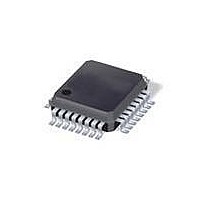
ATMEGA88PV-10AU Atmel, ATMEGA88PV-10AU Datasheet - Page 125

ATMEGA88PV-10AU
Manufacturer Part Number
ATMEGA88PV-10AU
Description
MCU AVR 8K ISP FLSH 10MHZ 32TQFP
Manufacturer
Atmel
Series
AVR® ATmegar
Specifications of ATMEGA88PV-10AU
Core Processor
AVR
Core Size
8-Bit
Speed
10MHz
Connectivity
I²C, SPI, UART/USART
Peripherals
Brown-out Detect/Reset, POR, PWM, WDT
Number Of I /o
23
Program Memory Size
8KB (4K x 16)
Program Memory Type
FLASH
Eeprom Size
512 x 8
Ram Size
1K x 8
Voltage - Supply (vcc/vdd)
1.8 V ~ 5.5 V
Data Converters
A/D 8x10b
Oscillator Type
Internal
Operating Temperature
-40°C ~ 85°C
Package / Case
32-TQFP, 32-VQFP
Processor Series
ATMEGA8x
Core
AVR8
Data Bus Width
8 bit
Data Ram Size
1 KB
Interface Type
SPI, TWI, UART
Maximum Clock Frequency
10 MHz
Number Of Programmable I/os
23
Number Of Timers
3
Operating Supply Voltage
1.8 V to 5.5 V
Maximum Operating Temperature
+ 85 C
Mounting Style
SMD/SMT
Minimum Operating Temperature
- 40 C
On-chip Adc
10 bit, 8 Channel
Package
32TQFP
Device Core
AVR
Family Name
ATmega
Maximum Speed
10 MHz
Controller Family/series
AVR MEGA
No. Of I/o's
23
Eeprom Memory Size
512Byte
Ram Memory Size
1KB
Cpu Speed
10MHz
Rohs Compliant
Yes
For Use With
ATAVRDRAGON - KIT DRAGON 32KB FLASH MEM AVRATAVRISP2 - PROGRAMMER AVR IN SYSTEM
Lead Free Status / RoHS Status
Lead free / RoHS Compliant
Available stocks
Company
Part Number
Manufacturer
Quantity
Price
- Current page: 125 of 420
- Download datasheet (9Mb)
8025L–AVR–7/10
The PWM resolution for fast PWM can be fixed to 8-, 9-, or 10-bit, or defined by either ICR1 or
OCR1A. The minimum resolution allowed is 2-bit (ICR1 or OCR1A set to 0x0003), and the max-
imum resolution is 16-bit (ICR1 or OCR1A set to MAX). The PWM resolution in bits can be
calculated by using the following equation:
In fast PWM mode the counter is incremented until the counter value matches either one of the
fixed values 0x00FF, 0x01FF, or 0x03FF (WGM13:0 = 5, 6, or 7), the value in ICR1 (WGM13:0 =
14), or the value in OCR1A (WGM13:0 = 15). The counter is then cleared at the following timer
clock cycle. The timing diagram for the fast PWM mode is shown in
shows fast PWM mode when OCR1A or ICR1 is used to define TOP. The TCNT1 value is in the
timing diagram shown as a histogram for illustrating the single-slope operation. The diagram
includes non-inverted and inverted PWM outputs. The small horizontal line marks on the TCNT1
slopes represent compare matches between OCR1x and TCNT1. The OC1x Interrupt Flag will
be set when a compare match occurs.
Figure 15-7. Fast PWM Mode, Timing Diagram
The Timer/Counter Overflow Flag (TOV1) is set each time the counter reaches TOP. In addition
the OC1A or ICF1 Flag is set at the same timer clock cycle as TOV1 is set when either OCR1A
or ICR1 is used for defining the TOP value. If one of the interrupts are enabled, the interrupt han-
dler routine can be used for updating the TOP and compare values.
When changing the TOP value the program must ensure that the new TOP value is higher or
equal to the value of all of the Compare Registers. If the TOP value is lower than any of the
Compare Registers, a compare match will never occur between the TCNT1 and the OCR1x.
Note that when using fixed TOP values the unused bits are masked to zero when any of the
OCR1x Registers are written.
The procedure for updating ICR1 differs from updating OCR1A when used for defining the TOP
value. The ICR1 Register is not double buffered. This means that if ICR1 is changed to a low
value when the counter is running with none or a low prescaler value, there is a risk that the new
ICR1 value written is lower than the current value of TCNT1. The result will then be that the
counter will miss the compare match at the TOP value. The counter will then have to count to the
MAX value (0xFFFF) and wrap around starting at 0x0000 before the compare match can occur.
The OCR1A Register however, is double buffered. This feature allows the OCR1A I/O location
TCNTn
OCnx
OCnx
Period
1
2
3
R
FPWM
4
=
5
log
---------------------------------- -
6
(
log
TOP
2 ( )
ATmega48P/88P/168P
7
+
1
)
8
Figure
OCRnx/TOP Update and
TOVn Interrupt Flag Set and
OCnA Interrupt Flag Set
or ICFn Interrupt Flag Set
(Interrupt on TOP)
(COMnx1:0 = 2)
(COMnx1:0 = 3)
15-7. The figure
125
Related parts for ATMEGA88PV-10AU
Image
Part Number
Description
Manufacturer
Datasheet
Request
R

Part Number:
Description:
Manufacturer:
Atmel Corporation
Datasheet:

Part Number:
Description:
MCU AVR 8K ISP FLSH 20MHZ 32TQFP
Manufacturer:
Atmel
Datasheet:

Part Number:
Description:
MCU AVR 8K ISP FLASH 20MHZ 32QFN
Manufacturer:
Atmel
Datasheet:

Part Number:
Description:
MCU AVR 8K ISP FLASH 20MHZ 28DIP
Manufacturer:
Atmel
Datasheet:

Part Number:
Description:
MCU AVR 8KB FLASH 20MHZ 32TQFP
Manufacturer:
Atmel
Datasheet:

Part Number:
Description:
MCU AVR 8KB FLASH 20MHZ 32QFN
Manufacturer:
Atmel
Datasheet:

Part Number:
Description:
Atmega88p 8-bit Microcontroller With 8k Bytes In-system Programmable Flash
Manufacturer:
ATMEL Corporation
Datasheet:

Part Number:
Description:
IC MCU AVR 8K 5V 20MHZ 32-TQFP
Manufacturer:
Atmel
Datasheet:

Part Number:
Description:
Manufacturer:
Atmel Corporation
Datasheet:

Part Number:
Description:
Manufacturer:
Atmel Corporation
Datasheet:

Part Number:
Description:
MCU AVR 8K FLASH 15MHZ 32-QFN
Manufacturer:
Atmel
Datasheet:

Part Number:
Description:
IC AVR MCU 8K 20MHZ 5V 32TQFP
Manufacturer:
Atmel
Datasheet:

Part Number:
Description:
IC AVR MCU 8K 20MHZ 5V 32-QFN
Manufacturer:
Atmel
Datasheet:


